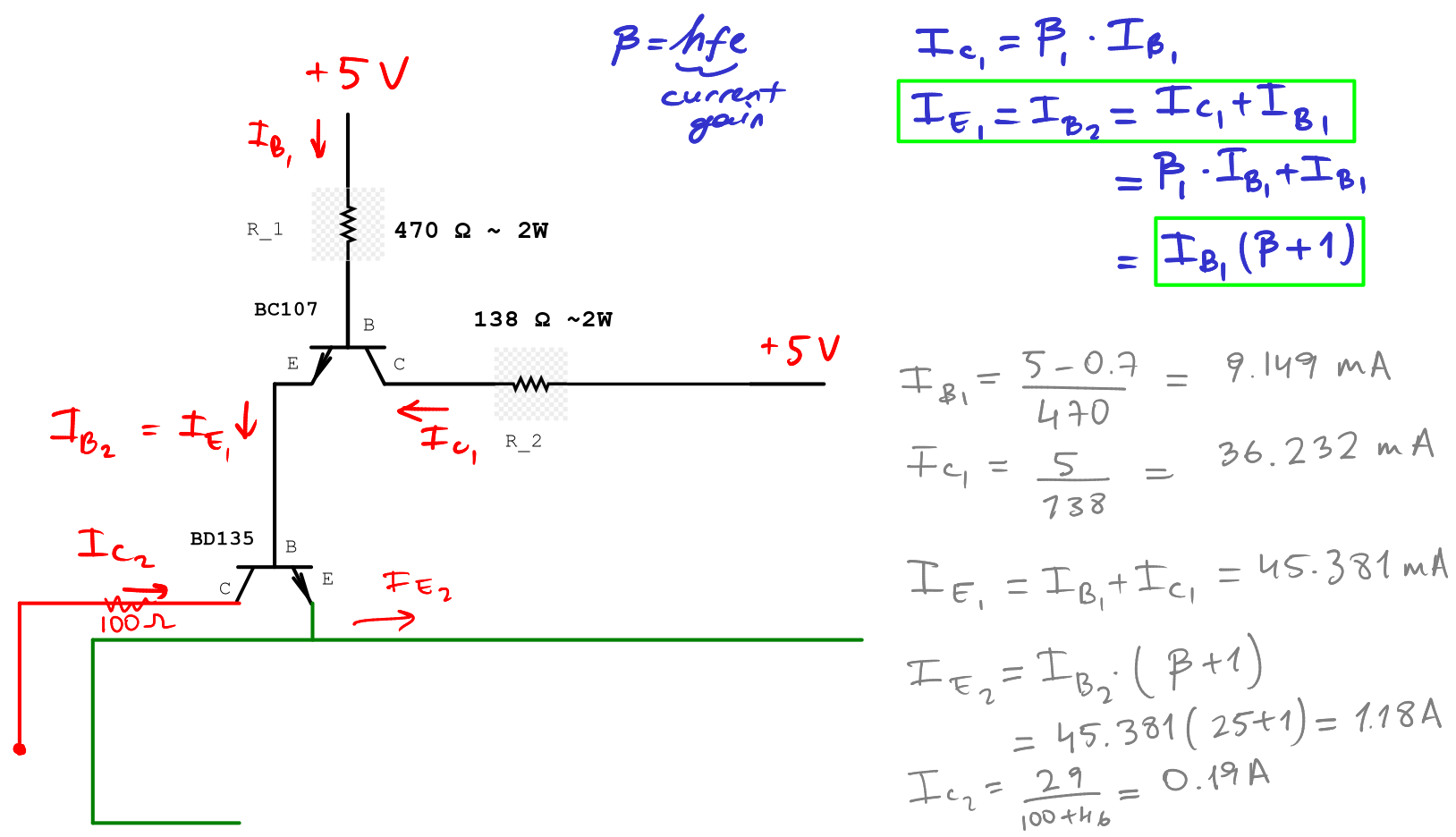
When you use the DB135 as a switch, power dissipation will be low:
Assumin a max. I
CE of 1.25 A (the limit of the transistor), the collector-emitter saturation voltage V
CEsat will be 0.25 V worst case (
datasheet).
The power dissipation is then P
CE = I
CE × V
CEsat = 1.5 A × 0.25 V = 0.375 W.
Add the power dissipatin from the base-emitter junction P
BE = V
BE × I
BE = 1 V × 0.03 A = 0.03 W.
The total power dissipation is then 0.4 W worst case (rounded).
The thermal resistance junction-ambient of the transistor is 100 ° /W. A power dissipation of 0.4 W will therefore increase the junction temperature over ambient by delta-T = 100 ° /W × 0.4 W = 40 °. Even when the transistor is operated in a hot environemnt, say + 40 °C, the junction temperature will be at max. 80 °C, way below the allowed 150 °C (max). Therefore no heat sink is necessary.
The heat sink you propose has a thermal resistance of 30 °/W. Add the thermal resistance junction-case of the BD135 you get a total of 40 °/W. The temperature rise from the dissipated power is then only delta-T = 40 °/W × 0.4 W = 16 °. This heatsink is absolutely sufficient in this switching application.

")