Maker Pro
Maker Pro

PCB building

Thank you very much. It actually is a stereo audio power amplifier 10 watt per channel (TDA2005).

I pulled the heatsink out of an old pc motherboard and i attached it with adhesive heatsink plaster.
 
Last edited:
just beware tho, in that latest board, you are still getting very close almost connections between lands and tracks that could lead to faults

Yes i am well aware of that. This is something i am working on. So far i had no actuall short circuit and no capacitance effect at AF and lower RF frequency range.
 
Here it is.
I've used different type connectors so i had to re-wire the whole box.
I've also used silicon wires that are much more durable and also resist solder iron burns.
The pins that are left blank are for future use with the "resistor-diode" array for RS232 communication. For now i use the Max3232 chip.
 

Attachments

  • IMG20160930_002.jpg
    IMG20160930_002.jpg
    130.3 KB · Views: 117
  • IMG20160930_004.jpg
    IMG20160930_004.jpg
    134.5 KB · Views: 105
  • IMG20160930_005.jpg
    IMG20160930_005.jpg
    90.9 KB · Views: 102
  • IMG20160930_006.jpg
    IMG20160930_006.jpg
    107.6 KB · Views: 105
  • IMG20160930_001.jpg
    IMG20160930_001.jpg
    83.6 KB · Views: 107
Last edited:
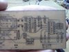
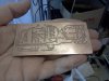
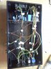
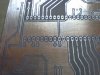
That board looks really good Constantine! I only see one trace that got necked down and needs rework. I got a roll of film recently and I am reading up on using the photoresist method. Alas, undercutting is always a problem with etching... The only way I have found useful to counter that is to take away as little copper as possible to form the traces and leaving the rest on the board. This may not be electrically acceptable in some cases, but for common circuits it should be ok. More environmentally friendly as well.
 
That board looks really good Constantine!.
thank you for being kind !

I only see one trace that got necked down and needs rework.

Yes i know. That happened because i left the board in the solution for too long. I am going to re build that board anyway because there are also a few changes in the circuit.

The new board will be perfect :)

The only way I have found useful to counter that is to take away as little copper as possible to form the traces and leaving the rest on the board.

I agree. That you can do by useing a not too strong solution.

This may not be electrically acceptable in some cases, but for common circuits it should be ok.

I guess you will have to try and see.
 
I agree. That you can do by useing a not too strong solution
I have found the opposite - if the solution is weak, it takes too long to etch everywhere evenly, leading to undercutting and pitting. A stronger solution in my recent experiences has successfully etched small boards (under 2"x2") in about 7 minutes. Warm solution works better. Having a denser toner transfer is crucial too, that is why I am interested in the photo method - I think that film will be more resilient and produce a cleaner etch.
 
I have practiced photo resist method for long time and i must say that exposure time in combination with the distance between the lamp and the board is critical as well as the quality of the printed transparency. It is better to print the transparency with an inkjet printer with as high resolution as possible otherwise UV light may destroy your board.
 
Here is the new board i made to replace the last one :)
 

Attachments

  • IMG20161109_002.jpg
    IMG20161109_002.jpg
    157.5 KB · Views: 118
  • IMG20161109_003.jpg
    IMG20161109_003.jpg
    141.8 KB · Views: 101
  • IMG20161109_004.jpg
    IMG20161109_004.jpg
    144.8 KB · Views: 109
  • IMG20161109_005.jpg
    IMG20161109_005.jpg
    133.5 KB · Views: 107
  • IMG20161109_007.jpg
    IMG20161109_007.jpg
    146.1 KB · Views: 102
Top