Maker Pro
Maker Pro

Chinese Hiland 0-30V/Audioguru PSU build (down the rabbit hole)

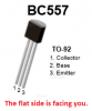
The BD139 is an NPN little power transistor that needs a heatsink and is Q2, not Q3. Q3 in the original project is a little BC557 or BC327 PNP transistor driven through R20 and it has a fairly low current to turn on the LED so it does not need a heatsink.
Maybe the Chinese kit labelled Q2 and Q3 differently to the original?

C8 connects to U3 pin 2, not pin 3. Maybe the Chinese kit has it going to the wrong pin?
 
Apologies:
This is what I should have said:

By swinging the Q3 (BC557CG) around I have it's base connected to R20 (30.1 & 1.79V) and then through C8(1.79 & 0.9V)to U2 pin3 at 0.9v

So either the drop through one of the components isn't big enough or I am starting off with too high a voltage.
 
But the bigger question is do I have the transistor the wrong way round.
Here is the transistor I'm using:

BC557
BC557.JPG
Am I correct in saying this view is with the flat side down ?

And here is what I think is a view of a 2SD9015

S9015.JPG

Now looking at them again, am I right in saying that the transistor pinouts are the same?
 
I looked in Google for BC557 and this is the first datasheet (it is from ON Semi) I found:
 

Attachments

  • BC557.png
    BC557.png
    14.6 KB · Views: 188
Your BC547 is made by a Chinese company so maybe their Engrish is too bad for them to say on their sketch "bottom view" or maybe it is a S9015 relabeled to show BC547.

Who cares about Q3? All it does is turn the LED on and off and it has nothing to do with the DC voltage at pin 2 of U3 being too high.
 
Am I reading your Rev 6 schematic correctly?

On the BC547:
Base is connected to R19, R20
Emitter to D13
Collector to R22
 
If Q3 is not the guilty party all that's left is incoming power:
D13: 41.6/31.6V
R19: 31.6/30.8V
R20: 30.8/ 1.7V
C8: 1.7/0.8V(normally 0.9V)

Who's on the firing line?
 
The inputs of U3 are pin 3 which is a voltage given by the current setting pot P2 and pin 2 which is a voltage from the project's output current sensing resistor R7. Since there is no load then pin 2 voltage should be almost zero and pin 3 voltage should be a little positive that causes the output pin 6 of U3 to go as high as it can which turns off Q3 and D9.

Something is causing the pin 2 voltage to be too high. U3 or C8 or a piece of conductive crud on the pcb.
Why do you say, "C8: 1.7/0.8V(normally 0.9V)" when the pin 2 of U3 end of C8 should be almost 0V and your 0.9V measurement is certainly not normal??
 
Still hunting for problems
Checking RV3 (100k pot) It reads from 0Ω to 30kΩ. Keep in mind that it's one leg is attached directly to one leg of R18 but I have attached probe between resistor and pot.
 
Why are you checking RV3? It controls the amount of maximum voltage set by the current setting pot P2 to pin 3 of U3 and its voltage was fine. But pin 2 voltage of U3 is wrong, not pin 3. With U3 removed then its pin 2 should measure 0V.
 
You said the B+ is 41.6V. Then if R1 is -5% its resistance is 2090 and it dissipates (41.6V squared)/2090 ohms= 0.83W.
Resistors are made to survive pretty high temperatures, your fingers aren't.
 
Still waiting for parts but I think this might help to point to problem areasAudioguru 0-30V Schematic Rev6 Jul 2014 D1.jpg
Voltages on either side of components.Some voltages could be transposed. Audioguru, I hope you can spot something that's been missed so far.

Please

Thanks
 
Top