1. Is the load circuit powered from a battery as designed?
Answer: I tried that and it made no difference.
2. Is there any other connection from the load circuit to mains earth, or to the power supply you are loading in the test?
Answer: I’m using a triple isolated output power supply, and I don’t believe there is load to earth.
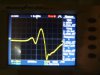
3. Can you see any waveform in the noise? Try the scope at different speeds and adjust the trigger threshold so it's within the noise.
Answer: Yes it’s a very nice sine wave, about 2uS See attached pix.
4. R3 and D2 are in the wrong place; they need to be between the collector of the current sink transistor and the input of the comparator, not between the collector and the power supply under test.
Answer: I think I fixed that see attached Schematic.
5. I assume that error is only present on the schematic, not on your prototype. Are there any other differences between the prototype and the schematic?
Answer: I hope not.
6. I would remove C2 (across the power supply under test). If you want to keep it in the circuit, at least test with it removed and see whether it makes any difference.
Answer: no difference.
7. Is the 11V rail clean?
Answer: Could be cleaner, I’ll test it with just batteries.
8. Is there any AC signal on the base of the current sink transistor?
Answer: No.
9. Have you connected a decoupling capacitor across the positive and negative power supply pins of the op-amp IC?
Answer: Yes .01uF
10. The op-amp is shown as two ICs, IC1 and IC2. I assume this is just another difference between the prototype and the schematic.
Answer: Yes, sorry I’ll fix that later
11. While you're at it, you might want to rotate Q3 clockwise 90 degrees. This just makes the schematic a bit clearer.
Answer

one
THANKS!