OK, here's what I've come up with.

This circuit must be powered from a clean, regulated 12V supply. It has an open collector output that goes low and latches low when the input voltage has remained between the two thresholds (1.3V and 0.7V) continuously for about 3.5 seconds.
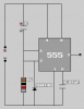
It is based around an LM339 quad comparator, U1, which is an old device but still widely used. The LM339 contains four identical voltage comparators, named U1A~U1D, which are represented as triangles on the schematic diagram, each with two inputs and one output.
Each comparator drives its output low if the voltage on its inverting ("-") input is higher than the voltage on its non-inverting ("+") input. If the "+" input voltage is higher than the "-" input voltage, the output floats and can be pulled up to a positive voltage.
This type of output is called "open collector". In the low state, it is able to pull down to 0V quite strongly, but in the high state, it does not pull up. External components must be used to pull the output up towards a positive voltage.
The input voltage is monitored by U1D and U1C, using two different voltage thresholds set up by the four-resistor voltage divider RA~RD. The voltages created by this voltage divider are marked on the diagram; these voltages are only accurate to within a few percent.
If the input voltage is higher than 1.3V, U1D will pull its output down to 0V. If the input voltage is lower than 0.7V, U1C will pull its output down to 0V. In either case, their commoned ouputs will pull to 0V and this will hold CT discharged, because QL is (initially at least) conducting like a short circuit.
Only if the input voltage is between those two voltage thresholds will both outputs go into the floating state, and allow CT to charge up through RT.
This configuration is called a "window comparator" because it compares the input voltage to a "window" between 0.7V and 1.3V. If the input voltage is outside that window, the commoned outputs pull low; if the input voltage is within the window, the combined output signal becomes "open" and no longer pulls down to 0V.
While the input voltage remains within the window, CT charges up through RT. If this condition remains true continuously, after about 3.5 seconds the voltage on CT will reach the 9.6V threshold voltage on pin 5. When this happens, U1A will pull its output to 0V.
When U1A's output goes low, QL turns OFF, and becomes an open circuit, and the commoned outputs of U1D and U1C can no longer discharge CT, even if the input voltage goes outside the input window.
Also when U1A's output goes low, U1B's "+" input goes lower than the fixed 9.6V threshold on its "-" input, so its output goes low as well. This output is designed to sink about 5 mA maximum.
Once the output goes low, it latches into that state. This is done by QL, a small-signal N-channel MOSFET, which is controlled by its gate, driven by the output of U1A. While the gate is high, i.e. +12V, QL will conduct when the window comparator's output goes low, and this will discharge CT. Once U1A's output has gone low, however, QL has no gate bias and does not conduct at all, so the window comparator cannot discharge CT. CT charges up to +12V and the circuit's output stays low until power is cycled.
I'm not too happy with this arrangement. If anyone can suggest a more reliable way, that doesn't require too many components, please do.
When power is removed and the +12V rail goes to 0V, DD conducts and discharges CT ready for the next run.
U1 is powered through pins 3 and 12 which are shown attached to U1A. CD is a 100 nF (also called 0.1 µF) ceramic capacitor called a "decoupling capacitor" and it is needed to ensure reliable operation of U1. It must be connected as closely and directly as possible between pins 3 and 12 of the IC - tacked on underneath the board is good.
DIN and RIN provide some protection against excessive voltage at the input.
CT needs to be a good quality low-leakage capacitor. Electrolytics might be suitable but I recommend a film capacitor such as
http://www.digikey.com/product-detail/en/R60DI4470AA30J/399-5908-ND/2571343
The delay time is determined by RT and CT. The formula is roughly
t = 1.6 × RT × CT
where t is the delay in seconds,
RT is in ohms,
and CT is in farads.
With the values given:
t = 1.6 × 470,000 × 4.7×10
-6
= 3.5 seconds.