Maker Pro
Maker Pro

Timing Circuit? Counter?

Hi Kris!

Quick question (I hope) :eek:

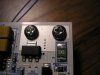
I'm looking at the voltage regulators you suggested and it appears (to me) that the tab is actually the voltage out line ?

I don't know if my understanding is correct but this is what I see;

Pin 1 = Ground
Pin 2 = Voltage Out (3.3 in this case) which is a trimmed leg (can't be connected)
Pin 3 = 12v IN

and then the tab is actually linked to Pin 2, or, voltage out (3.3v)

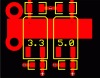
If my understanding is correct then, with respect to heat-sinking, I can't just punch down the tab to the ground plane of the board, which is what I was hoping to do. The idea being, spread the heat out over the entire ground plane.

I could be way off base with my understanding on how to work with these regulators. I was under the impression that the tab would be ground and that I could use a thermal via to connect it to the ground plane with the idea of using that as some form of board-wide heat sink.

Like I said, my understanding is limited :rolleyes: If my understanding is correct with respect to the tab actually being 3.3v out then what would be the best way to heat sink the regulator? It would seem to me that a 'normal' heat sink is not possible (ie. a bolt on aluminum piece). I attached a pic of the relevant section of the datasheet to save time.
 

Attachments

  • Picture3.jpg
    Picture3.jpg
    13 KB · Views: 120

KrisBlueNZ

Sadly passed away in 2015
You're right, on the AP1117, the tab is connected to VOUT. You can't spread the heat onto a groundplane. And you can't bolt it to an aluminium heatsink. You'll have to use a smaller "VCCplane". You can still put it on both sides and use thermal vias, though it might work out better to put it on the component side only.

You could look for a different, suitable linear regulator whose tab is either isolated or connected to 0V but I suspect you won't find one.

How much area can you spare for a VCCplane heatsink?
 
I did a search on VCCplane but did not have much luck other then I'm guessing you're suggesting making a surface layer heat sink in a similar fashion as this one on the daughtercard (see attached). At this stage in the board re-design I have a fair bit of room as I have left all the traces for last and am working on placement of components and circuit assemblies. Right now I have laid out the regulators side by side and they have a common ground on the caps. The caps are also very close to the regulator themselves (see other pic).

To specifically answer your question - I can add more space. The stock footprint for the 252-3 is oversize as it stands. I'm guessing the area in red on the footprint will come out as a copper plane?
 

Attachments

  • 1-P1010001.JPG
    1-P1010001.JPG
    35.3 KB · Views: 90
  • Picture9.jpg
    Picture9.jpg
    32.3 KB · Views: 86

KrisBlueNZ

Sadly passed away in 2015
Oops sorry for the confusion! "VCCplane" is what I would call a groundplane that's connected to VCC instead of ground! I just meant that you could add a copper fill, connected to VCC, for the purpose of heatsinking the regulator.

I would make it larger than the regulator's body outline, but I don't know how much you would need. I think it would also depend on whether there's a void in the solder mask for it. And I imagine that you could improve heatsinking by using thermal vias through to smaller areas on the underside that would interrupt the ground plane. I imagine there would be some thermal transfer between nearby vias, and between nearby copper as well, so you might be able to use the groundplane indirectly for heatsinking, but I don't know how effective that would be.

I'm kind of picturing an arrangement of vias and copper where the groundplane is electrically isolated from the tab, but coupled as closely as possible for the purposes of heat transfer, using closely positioned vias and/or copper areas. I would have to guess at the best pattern or arrangement to use for this, and I'm not sure it's even worthwhile. It's not something I have studied or experimented with.

I'm really just pulling ideas out of my arsenal at this point. See if you can find some proper advice online.
 
Yeah, it really sucks that the tab carries voltage out. If it were ground this would be very easy to punch the tab pad down to the entire ground plane on the board and use the whole thing for heat dissipation. That was my original plan.

The picture below should give me one giant wide pad on the top layer hopefully in a similar fashion to the one I pictured in post 44. The underside of the pic in post 44 also has a similar sized pad with 4 small vias to the backside pad. I'm a bit hesitant to create a similar sized pad underneath the top layer pad as it would be on the ground plane and I don't know how to electrically isolate it from the rest of the ground plane.

In the picture below, the two regulators are joined to one big pad. The two holes on the left are for mounting studs for a daughter board that are actually joined to the heat sink in the first picture in post 44. I think, electrically it will be OK but whether it will be OK with respect to heat dissipation is harder to say.

I could ditch the 3.3 volt regulator on the left and just use the 5 volt unit as the bluetooth module will run on 5V...I wonder if that might be smarter yet as it would result in less heat generation due to one less regulator...
 

Attachments

  • Picture37.gif
    Picture37.gif
    48.8 KB · Views: 91

KrisBlueNZ

Sadly passed away in 2015
Yeah. It's not unusual for components to have an inconvenient connection to the tab. Usually it's the collector or drain of the largest transistor or MOSFET in the device.

If you have a double sided board, and you just want a copper area on the underside that's connected through to the top side using thermal vias, you should just be able to create a copper area and the ground plane will "flow around' it. It depends on how the ground plane is handled by your PCB layout software. But there may not be any need.

Re removing the 3.3V regulator altogether. Assuming the Bluetooth module uses an internal supply rail of, say, 3.0V, it will have to drop the supply voltage down to that voltage, and it almost certainly doesn't have a switching regulator, so any heat you avoid dissipating by removing the 3.3V regulator will add to the heat that must be dissipated internally by the Bluetooth module anyway. I suspect that's why they recommend powering it from 3.3V instead of 5.0V.
 
That's what I did (if we're on the same page). What I did was create an oversize pad on the top layer that the regulator will sit on and an identical sized pad on the bottom layer (top and bottom of board). I then punched 4 vias through in a row in a similar fashion to the pic in the post above (#44). So, I should have a nice copper pad on the top and the bottom. If the bottom pad has 5V on it this won't matter, heck, I could even tap into it if I need 5V on the bottom in the future :D Some of this stuff, I'm just going to have to learn as I go, and when I have the proto boards in front of me I'll have a much better idea of what I did and what came out of it :eek:

I ran the BlueTooth module on my desk for a long while powered by 5V and it didn't even get warm. Based on that, I dropped the 3.3v regulator for the time being. I have space for it, actually, now that I've gone SMD I've got a decent amount of space left, but for simplicity's sake I'll leave it out for now. In addition, my second re-design is more dense and more logically laid out. It's not as sexy as version 1 but it's very, very functional :cool:

I'm getting much closer to pulling the trigger on having the prototype boards made....woohoo! ;)
 
Kris, I'm trying to lay out that circuit on my board - any chance you used a CAD package with an auto-router feature? I'd love to see a snapshot of what it came up with for a circuit layout on the PCB.
 

KrisBlueNZ

Sadly passed away in 2015
Well, I can generate a netlist for the connections in the schematic...

You would need to use the same component references as my schematic uses. You would need to translate the component type names to outlines, either manually or through a list, or place the components manually before you load the partial netlist and get your layout package to move the components based on the partial netlist (if it can do that), then auto-route that section.
 
Ah....I thought you just hit a button and it automagically generated a PCB layout. My software doesn't seem to have a proper auto router, which, I thought, just turned a schematic into a PCB layout using the most efficient trace layout. That's really what I wanted to see. I'm laying it out right now but it's not always easy for me to get my head around it. Just laying out my main PCB has been tough but it's pretty well done. I thought perhaps you just hit a button, take a screenshot, and away you go. Probably my unfamiliarity with the software is showing :)
 

KrisBlueNZ

Sadly passed away in 2015
No, there are several steps. It depends how tightly integrated the schematic and layout parts of the software are. If there is enough information in the schematic to specify the package, then the layout part can automatically choose and place the component outlines.

A netlist is a list of "nets"; each net is a list of {component, terminal} references that are connected together in one circuit node. The layout package uses the netlist to work out the best relative placement of the components, then to auto-route the connections once the components have been placed.

As I said, I can send you a netlist, but you would need to make the rest of the steps work.
 
It looks like my program (ExpressPCB) does have a netlist feature and linking of a schematic to the PCB editor...so I'm guessing it would work. Like I said though, I was under the impression it was an easy thing for you to do as I feel guilty about bugging you so much :)

If it's easy, by all means, please send over the netlist. Assuming I can get the autorouter (?) function to work it would be nice to see how they lay out the circuit on the PCB. It might even give me some interesting insights into how well I did with my layout of the entire board.
 

KrisBlueNZ

Sadly passed away in 2015
OK, here's a netlist giving the connections between the components in the diagram. It's in Tango format and it's readable. Each net starts with an open parenthesis on its own line, then a net name (which is just a number if no name is specifically given in the schematic), then one or more lines, each containing a circuit reference, a comma, and a terminal identifier, and identifying one connection point in that node. Here's net 4:
Code:
(
4
R1,2
DL,ANOD
U1,7
R2,1
)

The terminal names are as defined in the components in my schematic program. Resistors and capacitors have two pins, numbered 1 and 2; ICs also have numbered pins; diodes have two pins named ANOD and CATH. If your component outlines have pins with different names, you should edit the netlist before you load it.

Non-polarised components, and interchangeable elements within an IC,are not flagged in any special way, so you have to get resistors and unpolarised capacitors "round the right way" and you can't gate-swap.

Good luck!

Edit: oops! Forgot to attach the file! Remove the ".txt" extension.
 

Attachments

  • ep269993.net.txt
    457 bytes · Views: 158
Hahaha - thanks!!

I found an import netlist function in my PCB software and it gave me 4 options for different netlist formats. Unfortunately, none of them worked o_O
I then thought to myself, why don't I see if I can find the app you used to create it? It sounds like it was made with something called Tango. If that's correct it looks like it pre-dates the Internet and also the graphical operating system :D Now that's kickin' it Old School :)

Perhaps KiCad or Eagle can do it. I would really love to see an autorouter generated PCB of that circuit just to see how they would route it. It would probably give me a whole new way of thinking. NO worries, I'll dig into it. Thanks very much for providing the file and the explanation on how it's comprised!
 

KrisBlueNZ

Sadly passed away in 2015
No worries. I don't use Tango; just their netlist format. My EDA package (OrCAD/SDT III - yes, also very old-school) can generate lots of netlist formats. Give me a list of the formats supported by your PCB program and I'll see whether it can do them.
 
I was going to say...from the research I've done, if you were using Tango, you'd have to be about 105 (or so) and you avatar doesn't look a day over....27 :)

OK, the software natively supports netlist text files from;

Pads PCB
Pads 2000
Multiwire
ExpressPCB Netlist Text File (that makes sense given I'm using Express PCB) ;)
 
I'm also looking for a way to get it into Eagle & KiCad but not much success. Mind you, those programs are a lot harder to use then ExpressPCB
 
Last edited:

KrisBlueNZ

Sadly passed away in 2015
OK, OrCAD/SDT III's netlist program doesn't know about ExpressPCB (it wouldn't have existed back then) and it also can't do PADS (at least not under that name), but here's its attempt at a Multiwire netlist. Again, remove the .txt extension.
 

Attachments

  • ep269993.multiwire.net.txt
    2.4 KB · Views: 129
Interesting!

It does kaff on importing it with this error;

"Component Pin Number is not a Number. See Line 2"

The file looks pretty simple;

12V RA 1
12V DD CATH
12V RT 1
12V R1 1
12V U1 12
12V CD 1
2.495V RA 2
2.495V U2 3
2.495V RB 1
2.495V U2 1
2.495V U1 4
N00003 RT 2
N00003 DD ANOD
N00003 D1 ANOD
N00003 U1 6

So it looks like the import will fail on each line in the 3rd column that is not a pin number (ie, not numerical)
Can those be changed to pin numbers? If so, it will work! :)
 
Top