Well I didn't get all the captures I'd have liked. When I tested the "short circuit protection" by shorting the output, the fusible resistor opened, (I'd assume other components did as well.) So now I need to repair it before continuing. I should've left that test for the veeeery last. Hindsight, eh?
Some basic stats:
Load: 20W 16 Ohm non-inductive load resistor. (What I had handy for the output range, I really need a programmable load.)
Vout: 5.331Vdc
Iout: 330mA
Pout: 1.76W
Vopen(no load): 5.40Vdc
Vin: 120Vac
Iin: 42.5mA
Pin: 2.95W (real power)
Pin: 5.1VA (apparent power)
PwrFactor: 0.578
Efficiency: 59.66%
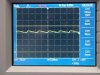
SwtchFreq: ~64kHz
I had expected a bit more efficiency from this thing... but, 60% sounds reasonable. (Edit: under full load, it may be better, I'd need to check that.)
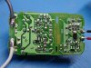
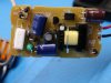
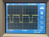
Anyhow! You can see how the AC input is being turned into Vbulk through the bridge and the caps. The inductor does nothing to smooth the ripple on top of Vbulk, since the Vbulk ripple is identical on both sides of it. I don't know if their intent was to try to smooth this ripple (like an LC PI filter?) or as a means to some type of DCM EMI filtering? (Though that would be on the other side of the bridge, yeah?) Seems pretty extraneous though.
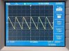
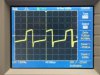
That Vbulk is turning Q1 on through the divider R9, R10, R11 and getting the switching started, (see Startup_Q1_base.) As the aux coil charges, he pulls Q1's base low through the RC network R7, C5 at ~64kHz (a very common switching frequency.) and the cycle repeats itself in a steady state. (see Q1_base.)
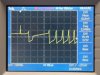
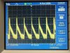
Primary current was measured across current sense resistor R4 (252mVpk, for a 115mApk primary current, see Primary_Current.) The rapid drop off of current leads me to believe the snubber is working overtime, but I didn't want to try to measure that without an HV probe. If I'm thinking right, we can see something like 600-800V+ spikes if the primary suddenly ceases all current flow, right? I don't want to replace my scope's front end just yet. Edit: Just sitting here and it popped in my head that I was reading across the current sense resistor for the primary current measurement... of course it drops off sharply, it's below the switch. When the switch opens, all current (through the resistor) ceases very rapidly. The current through the primary winding will ramp down at a normal rate, through the snubber... ugh, I'm losing it.
")
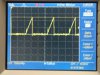
Anyway, when the primary collapses each cycle we get that energy induced into the secondary (see Vsecondary, which is the voltage directly across the secondary winding.) Notice it's ~24Vpp, most of which is negative, that's normal and familiar. Now normally, you'd see the catch diode (D9) first thing, right on the secondary output (pin 6 here.) They've put another catch diode on the negative side, D8, to allow C8 to act as the output bulk cap while still being west of D9. I've not seen this scheme before, and it's exact purpose eludes me... but it does appear to work. I contend that they could've saved themselves a diode by doing it the normal way.
Any thoughts?
R14,15,18,20 are forming a current sense resistor for the output (~2.02 Ohms) which is sensed by R19. This will bias Q3 to start turning the opto on when the current starts to get too high. That brings your duty cycle of Q1 down (lowering the output) via Q2. Though the fabled short-circuit protection still doesn't work, obviously, since I managed to smoke it. In any case, R21 and D7 form an OVP circuit, which DOES work quite well. Otherwise, everytime you unplugged your phone the supply would blow up. With no load, the supply's open voltage would raise quite a bit. I'm not sure what the zener's voltage is, it's a little SOD-323, so I can't even see the markings... (deduced he's a zener by measuring the voltage across it w/ load and without) but he starts to conduct whenever the voltage goes too high, which turns the duty cycle down through Q3, the opto, and Q2. This works quite well, as it limits the output to 5.4Vdc. I didn't get scope caps of that, but I did take a peek at the waveforms, and yes, Q1's duty cycle went down when I removed the load.
Now that's all well and dandy, that's a basic flyback. What still trips me up is the whole interaction between Q1, Q2 and the aux coil. I'll throw some guesses out there and see what you guys think:
I get that Q1 and Q2 form a current control scheme, that's pretty basic. R7 and C5 switch Q1 based on the TC, got that. D6 and R12 are shunting the negative spikes from the aux coil (like a snubber,) right? I guess my only confusion is R8. So is it some kind of pull-down for Q2? I take it it's weak enough to not disrupt Q1/Q2's steady state operation, but what purpose does it serve if it doesn't actively pull-down? (Actually I may have answered my own question... does it act as a divider for the opto, to establish the postive ~17Vdc coming from pin 4?) That may make sense, actually. I like it. I need to read up on the detailed operation inside the off-line controller ICs, to get a better feel of how exactly they are switching these things.
Ok, I've typed too much. I'm sure I've made some mistakes / assumptions which are untrue, but please do comment. Learning is my goal here, afterall.