Maker Pro
Maker Pro

Learning Kicad

This very quick video tutorial was useful and easy to follow,

Exporting images as SVG files to then convert to JPG or PNG to be able to share here via Imgur was a little tricky, . This quick video tutorial was helpful for this,
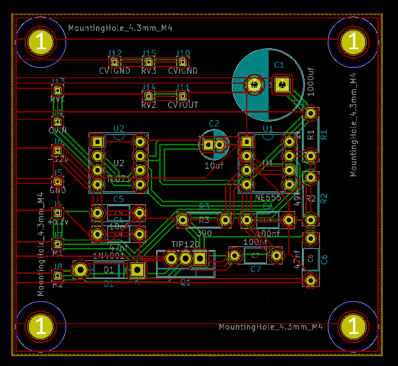
 
I usually place mounting holes in the corners.
Also no ground plane?
I use Greenshot for capturing JPG's.
M.
 
I usually place mounting holes in the corners.
Also no ground plane?
I use Greenshot for capturing JPG's.
M.
Ahh ok, I didn't realise I'd need to have a ground plane as all the ground connections are connected?

Yes, mounting holes! I'll add them, thanks, that would have been a really annoying thing to forget!

I'll look into Greenshot, thanks, "edit" I downloaded greenshot and it's perfect, thanks!

Darren
 
Ahh ok, I didn't realise I'd need to have a ground plane as all the ground connections are connected?
Darren

It is not compulsory ;)
But most cases advisable for most circuits..
Fortunately the one I forgot it on, was very low freq signals and minor circuitry.
M.
 
Ok thanks.

I'll try to add a ground plane as that is something else to learn, might as well fit as much learning in as possible o_O Also I'll do some reading about ground planes also

Darren
 
Hi, got back to kicad today.

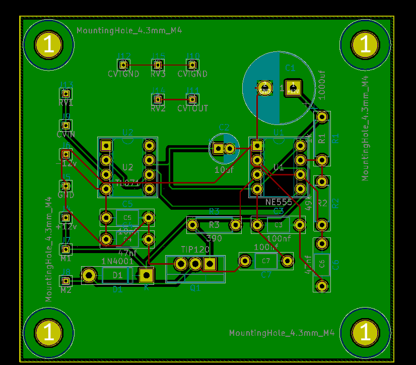
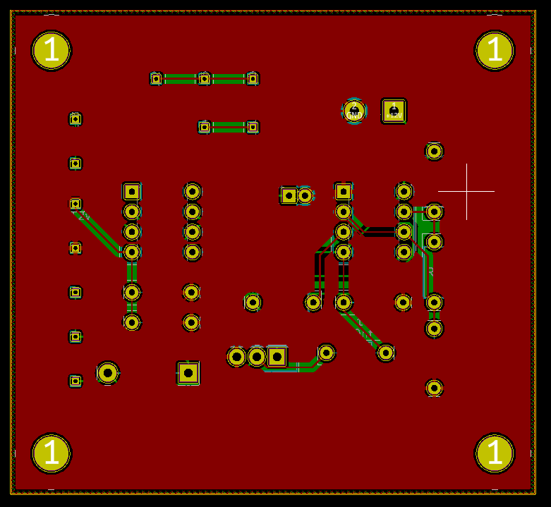
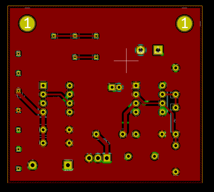
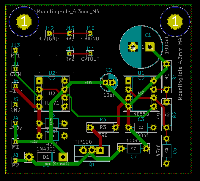
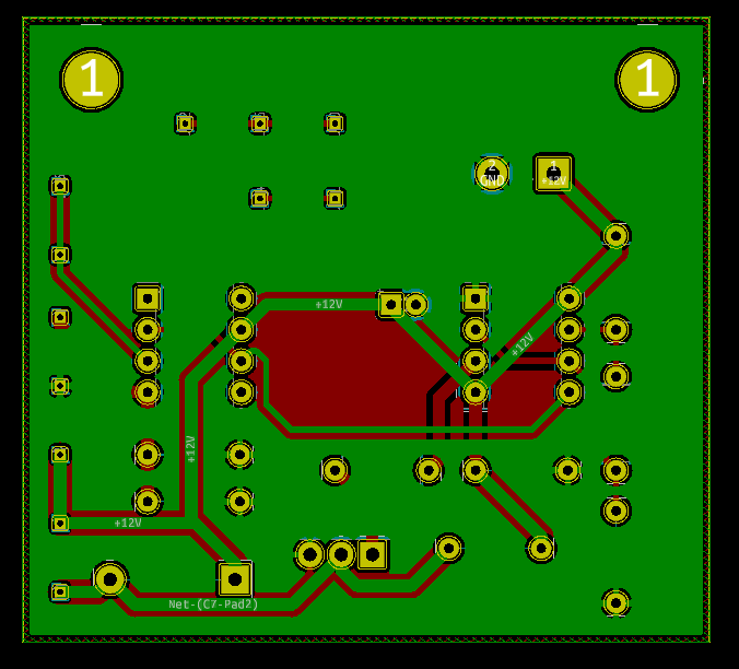
Here is how the ground planes and mounting holes are looking. I wasn't sure which image was needed, so posted three

This one is " Show outlines of filled areas only in zones"
MKwakhB.png


This one is the 'back layer' filled zone before i added the front layer

XVxtRZM.png


And here is the front layer's filled ground zone

KbY9YSa.png
 
One other thing I do when starting the PCB is to set the various trace widths up that I think I may need and then it is very easy to select them when running traces.
Larger for power etc.
M.
 
Hey M
Feel like i'm missing a hint here? Maybe the trace drawing current to the mosfet?

edit#

do the power traces need a larger width?
 
Last edited:
With the amount of real estate you have there, there is no reason to skimp, especially on the significant traces.!;)
M.
 
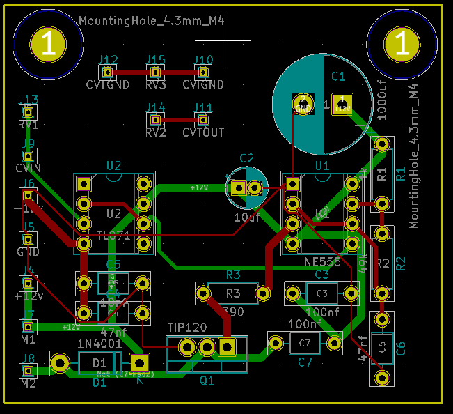
Here's the updated pcb new file without ground plane and new trace widths, I used an online calculator, https://www.7pcb.com/trace-width-calculator.php. The motors I am using have a stall current of 1.5a and the online calculator suggests a trace width of 0.942mm. I made the traces relating to TIP120/motor out all 1mm wide, and both the +12v and -12v supply lines.

I changed all other traces to 0.5mm, no other reason than 'not to skimp'. I couldn't find any online material that suggested the 3khz trace output of 555 needed a specific width, but then i'm certainly not fully understanding what I am reading, lot's of new terminology.

I also got rid of two of the mounting holes as I prefer to mount pcb's vertically

DVvI44A.png
 
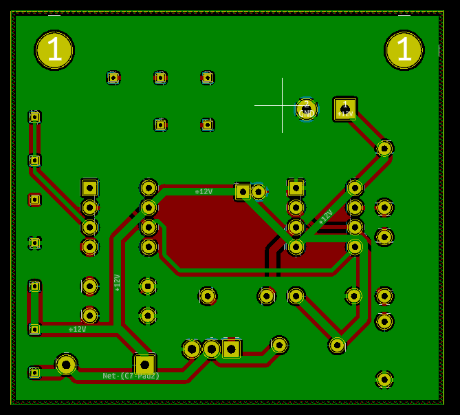
Ok that was a little easier than i thought it was going to be, just hadn't paid attention to traces being too close to pads as I'd relied too much on kicad deciding where the traces should go.

This passes the design rules check.

6Mz9x39.png


Rgc0mnN.png
 
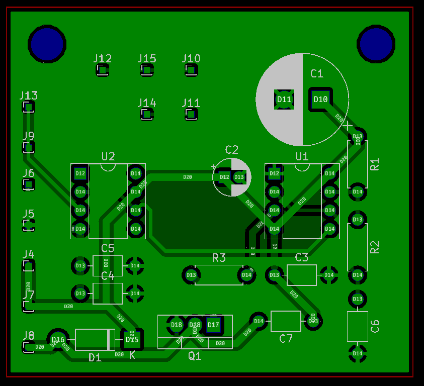
Am a little confused. How come in pcb view, when i select front view and front silkscreen layer i see all the text I'd like on the final pcb, but when i view in Gerber view I don't see all the texts, just the reference for each component?

pcb view

TVCirPO.png


Gerber view

rCve6it.png
 
The next step is to ZIP or RAR it and send to the board manuf, PCBway etc for their approval.
They will tell you if it comes up to scratch.
M.
 
Top