Maker Pro
Maker Pro

Digital programmable CDI ignition for 2-stroke engines

may 6
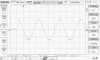
continuing with discovery via experimenting w/ the U4 4047 chip that is on the 2012 CDI PCB
the exp's are taking place on a bread board for now.
goal today = show what it means for the 4047 to operate in 'gatable' mode.
.............. plus 2 circuit examples that were wired up on a bd.bd and 'scoped.
............... there are many images that result from the experimenting.
............. as well as 3 TI 4047 data pages that refer to what is going on here.
... this all is to set the stage for my eventual goal of having the 4047 emit just one pulse.

... this one-pulse-at-a-time will be for more experimenting.

first image is p.1 of the data ... to highlight the gatable feature this chip comes with

may 6 4047 p.1.jpg

2'd image is p.2 of the data and the top-of-page table that shows us the connections to make
.................. for 'true gating' i.e. use pin 5 AST as the gating-pulse input and how we have
............... 3 pin choices where to take out gated clock output from : 10 , 11 or 13
... actually i'm not sure if pin13 , OSC, is gatable or not. it was not scoped

may 6 4047 p.2.jpg
 
Last edited:
may 6 ............ continuing ...
now a circuit sketch. this one uses a mechanical switch to create the AST gating
pulse . how did we get such a 'clean' AST signal using a switch ? they are known
to bounce for 1 to 10 ms . ??? oops, the AST signal was not scoped. so however it
looked on a scope the result is the Q pin output its signal with the LE of AST


may 6 4047 sw gating.jpg

and some screen shots. the 1'st is of a mis-wiring during exp'ing where even using
the correct pins i learned there are 2 ways to wire it. one of which is wrong

DS1Z_QuickPrint26.jpg

this next image was wired right. and Q pulses came out while the AST pin was a logic '1'

the Q pulses are a solid 'block' of ink as there are 1000's of them

DS1Z_QuickPrint27.jpg

i messed up by not including the incoming AST pulse from the switch circuit.
you'll see it though with the next set of images
 
Last edited:
may 6 ... continuing ...
here the mech'l switch is replaced with a pulse generator. now we can better control the on-time
of the AST pulse signal. plus we are not dealing with switch bounce anymore.
this is how we create an exact known quantity of Q output pulses.

note - if you dont have a pulse generator you can make up one by coding a 12F508 uC.
they are made to easily output pulses of width in the 1 to 256 us output range.
for either 'true gating' or 'complement gating'

may 6 4047 pulse gen_r gating.jpg

next is an image of just pin 10 Q clock signal at 100khz. the 4047 is in 'free running' mode.
at the image bottom can be read period = 10us and freq = 100khz


DS1Z_QuickPrint31.jpg

now we'll shift to gated mode and apply a series of AST pulses 65 , 28 and 8 us wide

DS1Z_QuickPrint40.jpg

DS1Z_QuickPrint40.jpg

DS1Z_QuickPrint41.jpg

DS1Z_QuickPrint42.jpg

this last one with AST = a 8us pulse and just one Q pulse output was my goal. earlier, non-posted,
experiments with the 3845 failed this step. oh , it did output just one pulse , only it was not
sync'd with the incoming trigger signal. the 3845 is not designed with a gatable output. what
you get is an output pulse in part or in full in the '1' on-time of the trig' signal.

sorry for the duplicate image. the system would not allow it to be deleted.
 
Last edited:
may 6 ... continuing ...
this last image shows us how the Q output follows the AST pulse leading edge. with some
delay. measured on my scope to be about 150ns.
at the bottom of p. 2 of the TI data , fig. 2 is a circuit sketch of the 4047 innards .
and on it i count about 9 logic gates/symbols in the path AST-to-Q. and every one adds
some delay from arrival of the AST LE input pulse to the Q's LE output pulse.
the total of all these delays is a spec' you can find on p.4 . they are shown for a V+ of
10 and 15 not the 12 my circuit was running at. anyway you can still get a ballpark
idea of what this total delay is.

DS1Z_QuickPrint43.jpg

this concludes today's posting of how to gate the 4047 clock output. we have achieved
controlling the width of AST to get just one Q pulse of 5us width output.
by changing the Rt and Ct values we change this single Q pulse width.
these single Q pulses will be at the center of the next set of experiments.
 
Last edited:
may 11
in order to more fully understand the CDI circuit we have to know what the signals on both sides of T1 are.
the operation of the DA-2033 Coilcraft transformer and the C2 cap is taking us all to the land of high voltages.
in the range 200 to 500+ V , both DC and AC.
and is calling for learning how to set up the Rigol 1054 scope to read them safely.
after all any scope has a maximum level of voltage on its input BNC terminals it can tolerate.

somewhere i got the idea that having an isolation transformer for probing circuits with
hi-V's in them made it safer. so a 300 watt one was bought at Amazon. for about $60.

next is to find a high voltage signal of known amplitude. then see what settings on the probe and scope
lead to showing what its value is. and keep playing with it all until the numbers agree.

one signal of known size is everywhere. at a nearby wall AC recepticle.
we call it 110VAC, or 117VAC too.
this is really the V-RMS of the Vpeak. and Vpeak is referenced to its 0 volts crossing point.
the sine signal has a peak in both directions ... positive & negative. and they are the same
for our domestic service.

on doing a Google search a a few minutes ago for "Vpp of household AC voltage"
here is some of what turned up ...

" Let's go over a real life example of VPP in an item you see regularly in buildings everywhere, including your home- an AC outlet. As you may know, an AC oulet outputs 120V. This voltage is not the peak-to-peak voltage. This is the RMS voltage. If you need an explanation of RMS voltage, see RMS Voltage and Current-Explained.. This same 120Vrms is 170V in peak voltage. So in peak-to-peak voltage, it is 340 volts. So the voltage which comes out of your AC outlet (United States) is 340Vpeak-to-peak. This is just a common example. "

so by placing the scope probe on the hot side of the wall recepticle you should see a 60hz sinewave
with Vpp amplitude in the 340V ballpark.

here's what i got : DS1Z_QuickPrint63.jpg

the same signal was gotten probing the 'neutral' wire off the iso'n txfr.
they are the same sinewave signal. just a half cycle out of phase w/ each other.

apparently an isolation txfr loses the incoming neutral AC line. and both rectangles
of the receptacle in which the plug goes are 'hot'

by reading the bottom line of the screen you'll fine Freq = 60.2 Hz & Vpp=368 V
other relevant info on the screen is along the R side ... Probe 20X
and again at the bottom how CH 4 is 100 V per division.
along the R edge of the screen signal grid is a T showing where the sinewave was
triggered. at the upper R corner see 92.0 V

on the left screen edge is a '4' ... this shows the 0-Volts ref'ce level for CH 4

the 'Probe 20X' is not understood. i expected 10X . so that the probe10:1 switch setting
multiplied by the scope setting the signal level internally at 10:1 too ----> 100V/div .

but if i select 10X then the screen V- readings are half size ... 92/184 not 184/368.

next i'll get out my 400V hi-V DC PS and see if it still works. and if it does dial it
up into the 200 + range and see what the scope settings have to be to read its Vp output.

another puzzling scope matter was changing the CH 4 'coupling' from AC to DC didnt
change the V-readings any.

first tho i'll sketch out a ckt diag to show you what the layout and connections are
for the AC measurements taken already today. this will let you see an isolation
transformer setup. in case they are new to you too.

may 11 iso txfr probe 110VAC.jpg
 
Last edited:
may 13
on the april 27 post was a list of 6 documents that go with the 2012 CDI design.
here is no. 3 . , the one titled 'capacative discharge pulser fun' . dr tony alfrey added it to his site
after the #108 2014 kit went on the market. what you see here are scans of the
original 3. p document from his site. and again , he is no longer with us.
and neither is his site. they're all gone with the wind.

the words in blue were links that would once take you to the sources he refers to.
being as they are now just scans they no longer work as links.
and the movie wont play either.

with all that i am still following thru with their posting. and allowing that you
will find value in them. sooner or later. whether you follow in dr tony's steps
and do the experimenting or not.

CDI fun p 1 of 3.jpg CDI fun p 2 of 3.jpg CDI fun p 3 of 3.jpg
 
Last edited:
p1 of 16  hi V pulsers.jpg p2 of 16  hi V pulsers.jpg p3 of 16  hi V pulsers.jpg p4  of 16  hi V pulsers.jpg p5  of 16  hi V pulsers.jpg p6  of 16  hi V pulsers.jpg

may 17
here are the 1'st 6 pages of item 6 in the list of documents posted on april 27.
the 16p. document covers the two types of 'high voltage pulsers' science kits
for hobbyists that dr alfrey was then marketing.

this first type is a present day version of a Kettering style
ignition system used in cars since 1910. these six pages cover the
original design and how it was since modified with transistors.

the last 10 pages will be posted over the next 3 days. they cover the
more modern CDI type of ignition circuit . his 2012 design that has been
the focus of our study for some time here on this forum.

my only copy was already heavily marked up in red ink. then scanned @ 300dpi in color.
and 'Paint' has been used to erase the marks and notes. not all of them though.
its a timely process. many remain.

one of you reading this who has some spare time and a steady hand is welcome
to finish the job
 
Last edited:
may 20
14 , 15 , 16
that's all of them

note too that this document has blue-text . these were once 'net links.

the p.8 reference to a future adaptive duty cycle design was never made.
nor was the p.12 "more robust and powerful version" ever made either.

the one thing he did do was to improve this design with a 2014 version.
which , among other things, has an input interface for external pulses to
cause the spark to fire.

a troubleshooting repair guide nor a set of circuit board operating signals
was never offered either. for that you're on your own.

my next post will cover how using 10:1 and 100:1 probes and a rigol 1054 scope
let you view and capture input signals in the 400 volt size.

and the next post after that will show how using this knowledge lets us see
the high-voltage circuit board action with Q2 , T1 and C2 .
 

Attachments

  • p14  of 16  hi V pulsers.jpg
    p14 of 16 hi V pulsers.jpg
    273.7 KB · Views: 71
  • p15  of 16  hi V pulsers.jpg
    p15 of 16 hi V pulsers.jpg
    194.5 KB · Views: 82
  • p16  of 16  hi V pulsers.jpg
    p16 of 16 hi V pulsers.jpg
    199.9 KB · Views: 69
Last edited:
We use something similar on model aircraft. It is a small device that uses a magnet on the prop shaft to trigger a Hall effect sensor and produces a healthy spark. The fit various spark plugs. The timing is automatically adjusted depending on engine speed. We pay about £40 to 50 in the UK. They range from single to multiple cylinder units.
Look up RCexl on the internet. They are probably available on ebay.
 
june 2
last month on may 11 was a posting to use the 1054 scope to measure high voltage AC .
one image posted was of the scope signal , showing Max =184 and Vpp = 368.
well and good. as this was in the ballpark of what was expected. the issue is seen
along the right side of the screen image , where it reads " Probe 20X " .

the scope probe used then was in the 10:1 switch position. so the scope Probe
setting should read true values in the same 10X . but it didnt. the Max & Vpp
numbers were right only when Probe = 20X

that has bugged me ever since. so today i went back for a repeat of it all.
and got the same numbers again. using the setup in the 2'd image
posted on that day.

then i had a new idea. to connect the scope probe across both AC HOT wires.
on doing this , and setting Probe to 10X numbers close to the earlier ones were
read. this image is posted here. 17.jpg ........ read Max = 164 & Vpp = 328

the first hookup image for today had left off the isolation parts : a 0.1u cap
and a 100k ohm resistor.

the connection scheme used today is believed to be the correct way
to measure AC voltages. namely to probe the lines with AC voltage on
them. and not probe the GND wire and either one of the AC wires.

be mindful of today's testing and that on may 11 of using an isolation txfr for both
the scope to be plugged into and the source of the AC signal measured.
 

Attachments

  • line AC iso txfr , 1054 10x probe june 2.jpg
    line AC iso txfr , 1054 10x probe june 2.jpg
    140.8 KB · Views: 73
  • june 2 ckt with isolation parts.jpg
    june 2 ckt with isolation parts.jpg
    116.4 KB · Views: 63
  • DS1Z_QuickPrint17.jpg
    DS1Z_QuickPrint17.jpg
    62.8 KB · Views: 95
Last edited:
june 2
it should be mentioned that the Rigol 1054 scope used for these experiments has a limit
for input voltage to any of its 4 ports. if you Google this topic you get that the total
DC and any AC riding along with it has to be less than about 400V.

be clear too that the probe itself has a Vmax rating

nothing on this was found in any of the documents that came with the scope.

an e-mail to the USA seller came back " 300V." plus he wanted to sell a special
probe to me for measurements at this level. instead i bought one off ebay
good to 2000V and comes at a fixed 100:1 for about $24. ppd

so , using the probe in the 10:1 position you are safe to 300V.
to apply a 400 V signal is risky. molded on the probe is 10X:300V , 1X:150V .
for these tests the same CH 4 was used. with the sense that if it is damaged
then only one channel of the four will have been lost. and so far after taking it
to 392V DC at 10:1 there were no sparks nor any smoke.
it still appears to work good as ever.

in the next post i'll include a sketch of how with the probe switch in 10:1 mode
the voltage at the scope end of the probe cable is 40V when the tip is at 400V.
 
Last edited:
View attachment 34418 View attachment 34418

june 5
the 2012 CDI design by dr alfrey is at the center of this ignition project effort.
and for the past several months i have been following in his footsteps by being
engaged w/ learning some PCB s/w . in order to know more of what all he had to learn


the immediate practical purpose is having the interface-signals-circuit made into a PCB.
see the post on p.8 7-24-16 and 8-5-16 . this board, shown below , is half the size of the CDI board.
and it will mount an inch above the CDI board on standoffs.

this post is to make mention of that effort. and to show a first design .
the '12 CDI board itself is being copied too.

given the enormity of the work doing those 2 designs & learning the s/w
i'm thinking about making it all be an Electronics Projects post separate from this one.
if this whole CDI Ignition project were a book the code, the circuits, and the PCB's
would all be separate chapters

also the EasyEDA.com s/w site offers the option to have your design project be public.
so others can access it to order boards as-is or to make their own changes .

last month , may '17 , my first design try was for the 74164 /8-leds circuit
you've seen on this forum. and 5 boards were ordered.
see the mar 7 post on p.10 earlier this year for their most recent post.
the '164 boards will arrive in a week or so. then be populated and tested. and
provide some valuable feedback for how well this first try design process worked.
so until its lessons are known no new boards will be ordered.
already i know that corner mounting holes were forgotten . this is a
minor mistake as the holes can be drilled by hand with the Drermel tool.

signals bd for 2012 CDI  june 4.jpg

U1 is the uC 12F508 ...... U2 is the 7432 OR gate and U3 the 7414 inverter.
P1 is the connector for the flywheel timing input signal.
and P2 is for the 3 wires that connect this board to the CDI board U2 chip.

not shown is the copper fill ground plane layer. having it shown makes it
harder to see the traces.

also the red traces are on the top layer, and blue on the bottom one.
 
Last edited:
June 7
returning to the 2'd June 2 post. and the matter of using the scope to probe hi-voltages.
lets first state why this has come up.

the 2012 CDI circuit takes 12V and via some switching action with Q2 and T1 boosts it to 300-400V on C2.

for the sake of knowing the switching circuit operation the desire is to scope the drains of both Q1 and Q2
during the charging of C2 step. and see what's going on & what we can make of it all.

first though we have to study our scope input spec's and the probe spec's too .
and make sure we aren't probing more voltage than they are designed to handle.

this info was cited in the first june 2 post. namely to keep the voltage on the scope
BNC ports < = 150V. the same as the probe spec in 1:1 switch position.
that spec is molded into the side of the 4 probes that came with the scope.

now the 10:1 switch position can have 300V at its tip. and this is OK , as its voltage-divider
action will reduce that to 30V. well under the 150V Max.

same with the 2000V 100:1 probe .. at most it will deliver 20V to the BNC port connector.
here is a sketch of voltages at each end of the probes. a photo too of each probe.
notice the yellow switch on the Rigol probes. its how you select 1:1 or 10:1


002.JPG


scope probes 10,100 to 1  June 5.jpg
 
Last edited:
Q1 Q2 V-max  June 7.jpg Q1 Q2 V-max  June 7.jpg
june 7
this above image is off the Q1 and Q2 data sheets. each of those n-FETs has a spec for the max
voltage between its drain and source.. exceed that and it could well have become damaged.

going into this study i hadnt yet caught on to what the data was telling me. my focus was
on knowing how to measure hi-V's with the scope without doing any harm to it or the probes.
what i didnt know was the absolute size of these hi-V's on the CDI PCB.
then , like just this week , it dawned on me the spec's for Q2 and Q1 are telling me the upper
end of the range they can be in. that and knowing the circuit has worked well for several years
now meant neither FET was being exposed to V's > the spec V-max of 100 & 500

the result was now knowing which probes to use on each of the drains of Q2 and Q1.
for Q2 , since its under 100V the Rigol probe in 10:1 mode will do.
and for Q1 the 2000V probe is called for. as the potential to encounter 500V is real.

in the 10:1 position the Rigol scope probe is good to 300V. and since R9 and R11 can be
set so C2 stops charging at 300V or less the Rigol probe could be used here.
 
Last edited:
june 7
along with using the correct probe to measure Q2 and Q1 we also have to tell the scope
what the V-ratio is . when we do this the scope automatically scales the on-screen
V-readings like V-max and Vpp to read like it were a voltmeter.

having the scope do the math saves us that step.

from the image of the scope screen below you can see there many V-ratios in the list.
the only ones i've used are 1X , 10X and 100X

DS1Z_QuickPrint3.jpg
 
Last edited:
june 7
last month while playing around with the CDI circuit i tried probing Q2's drain while it was
charging up C2. and got a rather clean image. its what you see below.

i believe now that something was done to the secondary side to disable the spark from firing.
removing the U1 chip would do the trick.
the assumption is that the ignition coil can scramble the PCB ground plane with surges of charge
when it fires. and that they will mess with the scope catching a clean signal on the FET

CH1 is of the U4 100khz sqr-wave signal that drives the gate of Q2. and turns it on for 5uS
then 5uS later turns it off for 5uS

CH2 is of a probe showing us the voltage action on the drain of Q2
see that the highest part of the drain signal is 5 divisions up . or 50V , and thus is well
under the 100V Max rating of Q2

this screen image is of just the primary side of T1 .
later this week the C2 side of the circuit will be probed as well.
so we can learn what they both look like. and try to figure out how to read
the energy transfer from one inductor of the coupled pair to the other

at the risk of being way off base here's my take on what it is telling us :
...... for the first 3uS the drain is ringing with the leakage inductor energy fading away.
then for the last 1.5 uS we see one large risen pulse to about 25V .
then it quickly ends with the FET turning off.
the T1 has a turns ratio of 10:1. so one can expect this 25V to become 250V
on the C2 side of the T1.

this will be something to look for when the drain of Q1 is probed.

one last thing to look at and think about is that the actual flyback action
we are after, changing the Vcc of 12V / 25V to 250V has to wait 3-4 uS until the primary
side leakage energy is dissipated

DS1Z_QuickPrint52.jpg
 
Last edited:
May 12
this is a follow up to the june 5 post. the first of its kind on making PCB's for the
two main circuits we are dealing with in this ignition project.

to clarify for those of you new to this post :
.. the two main circuits/PCBs for this ignition project are :
.... a. the 2012 CDI circuit board that turns 12V into 300V to drive the ignition coil
............... and
.................. b. the 'signals board' . that takes the flywheel signal, crunches it with a 12F508 uC , then emits a 'fire' pulse to the a. board when its time to fire the spark plug

shown on june 5 and today is the b. 'signals board'. PCB . its a work in progress.

that june 5 PCB design was ordered. EasyEda was having a $2/10-boards sale
over the weekend. so i jumped on it even tho not feeling 100% ok with the design.

the decision to post PCB work on this forum topic or start a new one is decided in favor
of keeping everything , code , circuits and PCBs here.

on one u-tube video about using EasyEda s/w the voice-over mentioned the automatic routing may happen with errors. and went on to demo how to wire the PCB parts by hand.

the june 5 circuit shown with wiring was done by hand at the schematic stage. then it
was converted to a PCB ( as shown ) and the final wiring done with 'auto routing'
the result is seen as red or blue trace lines connecting the parts.

that's what today's PCB image is on track for next. wiring the PCB parts together by hand.
first the parts are all laid out where they go.
being sure of placement is important as its a bunch of added work to make wiring changes.

however changing our minds happens . so one strategy is to repeatedly save the board along the way.
the s/w allows you to save distinct PCB version files as you move along.
you could have a new file after each part is wired.
so if you want to make a change you wont have to start completely over.

one thing here to point out is the 'footprint' for the transistors Q1,Q2 and Q3 does not come
with labels e , b, or c. so one has to go find the mfg'rs data sheet and see who is what.

there's likely a way to label these footprints then save them once in some user library.
then recall them later for use in a new circuit.

a bonus to wiring by hand on the s/w PCB editor canvas is being able to print out the image seen here today. and then taking a red pen and blue one and practicing wiring it on the paper.
red for the topside layer. and blue for the bottom

also the opto-isolator (OK1) in the june 5 was a 4N27. it has been replaced by a FOD814. U5.
its advantage is its a smaller 4-DIP pkg

some testing with a pulse generator , this new U5 part and the 2012 CDI circuit board was
done. and the spark fired with every push of the 'manual' pulse switch. this test also
verified the chosen 3-wire interface to the empty CDI board U5 socket via P2 worked.

this testing ought to and will get posted. its importance is in showing how one can interface
an external TTL 'fire' pulse to the 2012 CDI board. remember its designer , dr alfrey, sold it
for experimenting as is . and not directly for running gas engines. for doing that he left it up
to you to figure out the wiring connections.
in his later , 2014 design that change was made. and includes an input TTL pulse connector

june 12 scan EE pdf signals PCB w_ silk.jpg
 
Last edited:
Top