Maker Pro
Maker Pro

What holes to put electrolytic cap in

The problem is, the board has more than two holes where it is labled "C9" for the electrolytic power capacitor (rated to 25 V, I don't remember the capacitance at this second). One hole is labled "+", but there are 3 other holes in the circle labled "C9".

What does it mean? Why are there more than 2 holes in the circle labled "C9"? Which one do I use?
 

davenn

Moderator
who knows ???

show us a sharp well lit pic of the board so we can easily read the writing

Dave
 
Need a picture.
A lot of the boards I've seen make allowances for replacement caps of different physical
diameters. Older caps were usually larger than the new ones with better dielectrics.
some boards have a third thru-hole, for the smaller or larger cap diameter (the trace
between the two holes is tied together). Look at the back-side of the board and
see if that's the case. I think it happened when the transistion period started from the
old bigger electrolytics, when the newer smaller electrolytics started showing-up on
the market.
 

(*steve*)

¡sǝpodᴉʇuɐ ǝɥʇ ɹɐǝɥd
Moderator
It's possible the board has various holes to allow the use ov various different sized capacitors.

Have you checked to see if any of these pads are actually connected together (that would be the dead giveaway)

edit: *snap*, but way too late.
 
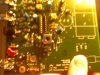
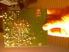
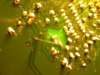
Attachment 33 - The whole board, right side up. The red thing in the bottom left is L5, the 13 turn VHF coil. In the bottom left you can also see Q1, the VHF transistor. In the center below the IC socket for IC U1., you can see L4, the shielded tuning transformer, that looks like a silver box with a screw driver hole on top to change the frequency of the local oscillator, it is labled on the board "FREQUENCY ADJUST". below L4, you can see C18, the 27pF cap for the modulation frequency near 88 MHZ. To the top right corner, you can see the 9 V battery silk screen drawing. To the top left corner, you can see (from bottom to top) DC input jack, RCA Right connector, and RCA Left connector. The the bottom left corner, to the right of Q1, the big silver circle surrounded by a green square is labled "ANT". To the extreme bottom left corner, you see the coax feed line connector. The things with yellow tops to the left of the IC socket are volume pots for Left and Right, R3 and R4. The thing with a yellow top to the right of the IC socket is a balance pot, R7. between the two blue painted electroytic caps in the top left corner is X1, the "silver can" 38KHZ crystal that creates the stereo pilot tone and stereo carrier frequency. To the immediate left of the two volume pots, you can see 2 resistors, R1 and R2, those attenuate the audio from line-level to a safe level for the IC. Immediately below the two blue electrolytic caps, you see two resistor and ceramic cap pairs which set the pre-emphasis. In the far bottom right corner, is S1, a push-pull power switch which I didn't put in yet.

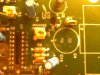
Attachment 33a - Zoomed into C4, next to the IC socket for U1. (The capacitor in question is C4, not C9 actually, and it is 1000 uF.)

Attachment 34 - Zoomed in more to C4.

Attachment 34a - Another angle looking at C4.

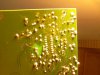
Attachment 35 - The whole board, upside down, without the cap in.

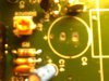
Attachment 35a - The board upside down zoomed into C4, next to the IC socket for U1, without the cap in.

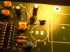
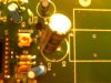
Attachment 36 - Putting the cap in the board. You can see VR1, what looks like a transistor but isn't, to the 11'O Clock of the cap C4.

Attachment 36a - Part of the board closer to C4, upside down board with the cap leads sticking out.

Attachment 37 - The board upside down zoomed in more to C4, with the cap leads sticking out.

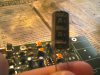
Attachment 31 - The cap itself, C4, 1000 uF, rated to 25 V. You can see the line-level lowering resistors R1 and R2. You see the empty spots for L1 and L2 that I didn't put in yet, because the kit didn't have them and Radio Shack doesn't sell inductors. L1 and L2 are for removing radio frequencies from the audio cables. There is also an L3 for providing a clean power supply, which I didn't put in L3 yet either.

I didn't put the IC U1 in the IC socket yet. The instruction manual in the kit says the IC is the LAST thing that you put in, probably because its the most fragile part and most expensive part.
 

Attachments

  • 0110141433.jpg
    0110141433.jpg
    52.3 KB · Views: 142
  • 0110141433a.jpg
    0110141433a.jpg
    42.6 KB · Views: 128
  • 0110141434.jpg
    0110141434.jpg
    38.1 KB · Views: 130
  • 0110141434a.jpg
    0110141434a.jpg
    41.7 KB · Views: 132
  • 0110141435.jpg
    0110141435.jpg
    48.8 KB · Views: 146
  • 0110141435a.jpg
    0110141435a.jpg
    37.3 KB · Views: 135
  • 0110141436.jpg
    0110141436.jpg
    41.2 KB · Views: 138
  • 0110141436a.jpg
    0110141436a.jpg
    48.5 KB · Views: 149
  • 0110141437.jpg
    0110141437.jpg
    43 KB · Views: 150
  • 0110141431.jpg
    0110141431.jpg
    51.5 KB · Views: 138
Last edited:

davenn

Moderator
I did tell you sharp aand well lit pics

but through the blurryness its the 2 larger centre holes you shoukl be using
you pic shows your mounting of the capacitor incorrectly
the 2 small holes on the edge of the circle are called via holes.
In this case they are connecting the top and bottom groundplanes

NOTE how the large centre hole ( the one closest to the + symbol) is isolated from the surrounding groundplane ! -- this is the hole that the + leg of the capacitor should be going through

Dave
 
Last edited:

(*steve*)

¡sǝpodᴉʇuɐ ǝɥʇ ɹɐǝɥd
Moderator
Is picture 37 showing your soldering?

Of I were you, I'd be practicing my technique. Whilst the photos are too bad to see if any of those joints are bad, there would be a lot to inspect...

Given that there is not a lot of space between some f the tracls etc, it might be worth posting a good sharp photo of your soldering so we can take a closer look and recommend any remedial action which might be wise to take.

Is this the first think you've built?

I think you may be using to much solder, too thick solder, too large an iron, or possibly a combination of all of these. If it's the case, it's not an insurmountable problem, but it does make it harder to get a good looking result.

The photo needs to be sharp, and taken with indirect light (in shade, for example) and NOT with a flash. If you're using a phone, place the board on a surface (i.e. NOT in your hand) and steady the shone by resting your hand or the phone on something.
 
Okay I will put it in those two center holes. Thanks for response.

Yes this is the first thing I've built.

Yes these pictures were taken with a phone.

Okay I will take a few photos of the soldering in the manner you recommend.
 

(*steve*)

¡sǝpodᴉʇuɐ ǝɥʇ ɹɐǝɥd
Moderator
When you're shooting from a phone, it can help t hold a "close-up" filter in front of the lens of the camera.

I have a camera with a *very* wide angle lens, and with a +4 close-up lens I took a picture of the back of my hand like this:

attachment.php


That's hand held, detailed, and sharp.

Listen to me. I know this stuff like the back of my hand.
 

Attachments

  • WP_20140101_00_10_29_Pro (Medium).jpg
    WP_20140101_00_10_29_Pro (Medium).jpg
    103.8 KB · Views: 197
When you're shooting from a phone, it can help t hold a "close-up" filter in front of the lens of the camera.

I have a camera with a *very* wide angle lens, and with a +4 close-up lens

Okay, I won't proceed with this project until I buy a 4x close-up lens to hold in front of my phone so you can look over my soldering before I connect the 9 volt battery and smell smoke.

No, I did not connect the 9 volt battery yet.

You may remember from my previous forays, that I have a tendancy of causing electronics to smoke, so that is a high probability with this project if you don't look it over.

Oh, and thanks for all of your time offering to look over my soldering.
 
Top