Maker Pro
Maker Pro

Theory of operation of MS3110 high resolution capacitive sensor

I am going to use the MS3110 to measure capacitance in a MEMS device, below is the function block diagram of this chip.
upload_2014-10-20_22-44-10.png
and the transfer function of this circuit is
upload_2014-10-20_22-45-35.png
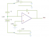
I tried to derive the transfer function, but I met a problem which is that I think amplifier here is used as an integrator, the noninverting input and inverting input of the amplifier should have the same potential which is 2.25V, but the inverting input is also determined by the capacitor array on the left side of the diagram, I was stuck here, hope anyone could help me with the derivation of the transfer function. Thanks!
 

Attachments

  • MS3110 datasheet.pdf
    891.4 KB · Views: 336

Harald Kapp

Moderator
Moderator
You're right, zhe opamp is used as an integrator.
For the purpose of analysis start by simplifying the circuit: replace CS1N || CS1 by Cx, CS2N ||CS2 by Cy.
Use the standard derivation of an integrator's transfer function. Assume that the voltage at the "-" input is the same as the voltage at the "+" input (V+ - V- = 0V). This is what the operational amplifier will try to achieve by adjusting its output voltage (Vout = A*(V+ -V-) and since A is on the order of 10000 or more, this will lead to (V+ - V-) ~ 0V)
The standard derivation of an integrator's transfer function uses the identity Iin = Vin/Rin. Since this circuit has no Rin (negligible small wire impedances neglected), how can you derive Iin from the capacitances (or the change in capacitance) and the available voltages? Hint: I(c)=f(V,C). Use this current as input to the integrator.
 
I don't believe you are given enough information to derive the transfer function. The input is a change in capacitance and the output is a voltage. But this is a switched capacitor circuit where the capacitors are switched between Vneg and a 2.25V reference voltage under some sort of timing control. I could not find any information in the datasheet regarding the details of this switching function. Or is the purpose of the analysis to determine by implication what this switching function might actually be?
 
I don't believe you are given enough information to derive the transfer function. The input is a change in capacitance and the output is a voltage. But this is a switched capacitor circuit where the capacitors are switched between Vneg and a 2.25V reference voltage under some sort of timing control. I could not find any information in the datasheet regarding the details of this switching function. Or is the purpose of the analysis to determine by implication what this switching function might actually be?
The purpose of the analysis is to understand the principle of operation in order to better use it. Would you please tell me how can you tell this is a switched capacitor circuit? Because in the diagram we could see any switch. Does it from the V2P25/VNEG? Could you please tell me what is the meaning of V2P25/VNEG? What's the difference between it and only V2P25? Thanks.
 
Here is the portion of the datasheet block diagram with the switching portion highlighted.

On the physical package there are multiple pin-outs for VNEG shown which suggests that VNEG is the system ground.

Untitled 1.jpg
 
You're right, zhe opamp is used as an integrator.
For the purpose of analysis start by simplifying the circuit: replace CS1N || CS1 by Cx, CS2N ||CS2 by Cy.
Use the standard derivation of an integrator's transfer function. Assume that the voltage at the "-" input is the same as the voltage at the "+" input (V+ - V- = 0V). This is what the operational amplifier will try to achieve by adjusting its output voltage (Vout = A*(V+ -V-) and since A is on the order of 10000 or more, this will lead to (V+ - V-) ~ 0V)
The standard derivation of an integrator's transfer function uses the identity Iin = Vin/Rin. Since this circuit has no Rin (negligible small wire impedances neglected), how can you derive Iin from the capacitances (or the change in capacitance) and the available voltages? Hint: I(c)=f(V,C). Use this current as input to the integrator.
According to what you said, the problem can be simplified as the following,
upload_2014-10-21_14-39-42.png
Here we make several simplifications
1. V+ = V- = 2.25V which is also the node1's potential since no resistor between node1 and noninverting input.
2. CS1N || CS1 = CS1N + CS1 = Cx ; CS2N // CS2 =CS2N +CS2 = Cy
3. The two voltage source can be simplified as two square wave between 2.25V and 0V, 180 degree out of phase with each other.
my idea is :
when the upper source is 2.25V, the lower source will be 0V, so the potential difference or voltage on Cx is 0V while voltage on Cy is 2.25V. Vice versa, when the voltage on Cx is 2.25V, the voltage on Cy will be 0V. In other words, when Cx is charging, Cy is discharging. That's all I can think of now. Would you please tell me how to calculate the current?

PS: I am a mechanical engineering student currently working on a project which involves using MS3110, this is not my homework, the thread was moved by editor to this section.
 

Harald Kapp

Moderator
Moderator
PS: I am a mechanical engineering student currently working on a project which involves using MS3110, this is not my homework, the thread was moved by editor to this section.
Sorry, that was my deed. Your post loked so much like homework. No offense meant.

I didn't see the switched voltages until Laplace pointed to this fact. Originally I was thinking that the change in capacitance id the effect that is evaluated. The basic equation describing current through a capacitor is I= C*dV/dt (fixed C) or I=V*dC/dt.

I don't think the switch between V2P25 and VNEG is intended to do the actual measurement. My idea is that it is intended to cancel possible asymmetries, but I may be wrong here as I'm not familiar with the circuit. But switching the capacitors from V2P25 to VEG and vice versa will lead to a rather high current spike (as dV/dt is very high) which I think is not well defined and therefore not suited for measuring the capacitance.
Assuming my theory is correct, one could analyze the circuit by assuming fixed levels either V2P25 or VNEG at the capacitors and lok only for changes in capacitance.

Any other ideas are welcome.
 
Here is the portion of the datasheet block diagram with the switching portion highlighted.

On the physical package there are multiple pin-outs for VNEG shown which suggests that VNEG is the system ground.

View attachment 16187
Yeah, you are right. It is a switched circuit and from other material I know that the frequency of open and close the switch is 100KHz. I think the center of the capacitor bridge is kept at 2.25V and and the capacitors on the two sides of center are alternatively charge and discharge, just like a switch circuit. I wonder do you agree with the center of capacitor bridge is kept at 2.25V?

Sorry, that was my deed. Your post loked so much like homework. No offense meant.

I didn't see the switched voltages until Laplace pointed to this fact. Originally I was thinking that the change in capacitance id the effect that is evaluated. The basic equation describing current through a capacitor is I= C*dV/dt (fixed C) or I=V*dC/dt.

I don't think the switch between V2P25 and VNEG is intended to do the actual measurement. My idea is that it is intended to cancel possible asymmetries, but I may be wrong here as I'm not familiar with the circuit. But switching the capacitors from V2P25 to VEG and vice versa will lead to a rather high current spike (as dV/dt is very high) which I think is not well defined and therefore not suited for measuring the capacitance.
Assuming my theory is correct, one could analyze the circuit by assuming fixed levels either V2P25 or VNEG at the capacitors and lok only for changes in capacitance.

Any other ideas are welcome.
Thanks for your reply. One thing I am pretty sure is the circuit must work under alternative voltage actuation, and it is used for capacitance difference measurement as indicated in transfer function, but the difference doesn't vary with time, so dC/dt=0. Anyway, you provide an idea that I never thought before which is the center of capacitor bridge is keep at 2.25V. Thanks for that.
 
Last edited:
Here is the portion of the datasheet block diagram with the switching portion highlighted.

On the physical package there are multiple pin-outs for VNEG shown which suggests that VNEG is the system ground.

View attachment 16187
Hi Laplace,

I learnt some basic switch circuit and found that a capacitor(C) in a switch circuit is equal to a resistor having a resistance of R=T/C, T is the switching period.
So when the upper source is 2.25V, the lower source is 0V, we have a simplified circuit like the following:
upload_2014-10-21_16-36-52.png
Current flow from high potential to low potential(p3 to p2), i=2.25/R2;
when the upper source has 0V and lower source has 2.25V,
upload_2014-10-21_16-38-47.png
Current flow from p3 to p1, i = 2.25/R1;
Supposing the simplest situation, R1=R2, then we have a constant current flowing through feedback capacitor Cf, we know that i = Cf*d(Vout-2.25)/dt, from this equation, Vout will become bigger and bigger as time goes by, that definitely is not the real case. What do you think?
 
I will use MS3110 to measure tiny capacitance difference in a MEMS device. For better use it, I try to understand the theory of operation. Could anyone tell me how to understand the MS3110 IC's circuit?
upload_2014-10-22_9-31-34.png
Transfer function
upload_2014-10-22_9-32-45.png
I have some idea after studying and discussing with others.
1. CS1IN//CS1=CS1IN + CS2IN=CS1T CS2IN/CS2=CS2IN+CS2=CS2T
so the capacitor bridge on the left side can be simplified as two capacitors,CS1T and CS2T, connected in series.

2. A clearer diagram of the two sources is shown below,
upload_2014-10-22_9-42-7.png
The two switches are 180 degree out of phase. When the upper switch connects to 2.25V, the lower switch connects to 0V, vice versa.
I thought this may be considered as switch circuit, and a capacitor in a switch circuit can be consider as a resistor with resistance R=1/Cf, f is the switching frequency.
So the circuit can be further simplified as 2 resistors connected in series.

3. The noninverting input of the amplifier V+ is equal to the inverting input V-, ie; V+=V-=2.25V.
So the center of the capacitor bridge has the same potential with V-, which is 2.25V.

The final version of simplified circuit is like below.
when the upper source is 2.25V, the lower source is 0V, we have a simplified circuit like the following:
upload_2014-10-21_16-36-52-png.16198

Current flow from high potential to low potential(p3 to p2), i=2.25/R2;
when the upper source has 0V and lower source has 2.25V,
upload_2014-10-21_16-38-47-png.16199

Current flow from p3 to p1, i = 2.25/R1;
Suppose the simplest situation, R1=R2, then we have a constant current flowing through feedback capacitor Cf , we know that i = Cf*d(Vout-2.25)/dt, from this equation, Vout will become bigger and bigger as time goes by, that definitely is not the real case.The amplifier should output a constant voltage, like shown in the transfer function. I think I must done something wrong. Hope anyone could point out my mistake.
 

Attachments

  • MS3110 datasheet.pdf
    891.4 KB · Views: 116
As you know the available explanation of the MS3110 theory of operation is rather sparse. But it does refer to a capacitive trans-impedance amplifier, although it is not clear how switching the voltage polarity across the sense capacitor is current-limited. What is not clear is how timing control of the voltage switching is related to resetting the feedback capacitor and at what point in the timing cycle the sampling for the sample-and-hold circuit is accomplished. All that is really known is that the output voltage is proportional to the imbalance between the sense capacitors. It may be that the sample-and-hold circuit is responsible for the constant output voltage because it periodically samples a changing amplifier voltage at the same point.

Screenshot-35.png
 
As you know the available explanation of the MS3110 theory of operation is rather sparse. But it does refer to a capacitive trans-impedance amplifier, although it is not clear how switching the voltage polarity across the sense capacitor is current-limited. What is not clear is how timing control of the voltage switching is related to resetting the feedback capacitor and at what point in the timing cycle the sampling for the sample-and-hold circuit is accomplished. All that is really known is that the output voltage is proportional to the imbalance between the sense capacitors. It may be that the sample-and-hold circuit is responsible for the constant output voltage because it periodically samples a changing amplifier voltage at the same point.

View attachment 16230
I think now I understand the operation of this circuit relies on timing control.Maybe it's not practical for me to derive the transfer function. I still want to know do you think my analysis shown above is right? especially the capacitive switch circuit part? In this circuit, can the capacitor be considered as a resistor? Thanks!
 
As you know the available explanation of the MS3110 theory of operation is rather sparse. But it does refer to a capacitive trans-impedance amplifier, although it is not clear how switching the voltage polarity across the sense capacitor is current-limited. What is not clear is how timing control of the voltage switching is related to resetting the feedback capacitor and at what point in the timing cycle the sampling for the sample-and-hold circuit is accomplished. All that is really known is that the output voltage is proportional to the imbalance between the sense capacitors. It may be that the sample-and-hold circuit is responsible for the constant output voltage because it periodically samples a changing amplifier voltage at the same point.

View attachment 16230
Hi Laplace,

Please check my latest explanation. I think perhaps we can derive the transfer function without knowing the timing information.

When S1 is connected to 2.25V, S2 connected to ground, C1 has 0 potential difference, according to Q=CV, there should be no charge on the C1 parallel plate. C2 has potential difference of 2.25V, so
positive charge with amount of C2*2.25 accumulate on the upper plate of C2 while same amount negative charge accumulate on the lower plate. Positive charge on the upper plate is the result of same amount electrons leave the upper plate, these electrons can only move to the left plate of Cf since C1 has no charge accumulated, so the potential difference Vout - 2.25 = C2*2.25/Cf.
upload_2014-10-23_16-31-27.png
When S1 is connected to ground,S2 is connected to 2.25V, then C2 has no 2.25-2.25 = 0V, so no charge accumulation on the parallel plates of C2. C1 accumulate charge with amount of 2.25*C1, Cf has correspondingly same amount charge which led to Vout = 2.25*C1/Cf + 2.25.
upload_2014-10-23_16-31-59.png
If my analysis is reasonable, the output voltage should be a square wave, but in the MS3110 datasheet, the output is a DC voltage as the transfer function shows.

I wonder why the output voltage is propotional to capacitance difference (CS1T-CS2T in the simplified version is C1 -C2)?
And where is the 1.14 term come from? Does it come from the low pass filter?
 
Last edited:
Hi,

I am working on MS3110, a high resolution capacitive readout sensor.
Here is the simplified circuit for MS3110.
upload_2014-10-23_15-13-58.png
The two switches are 180 degree out of phase, ie. S1 connect to 2.25V, S2 connect to ground.
The switching frequency is f.
After discussing with others, we think theory of operation of this circuit is:
The circuit generates a pulse of charge through the capacitors when the voltage is switched by the two switches, with the amount of charge at the op amp input proportional to the voltage step and the capacitance difference. This charge is integrated by the integrator to give a step voltage. The continuous switching of the switches gives a square-wave step at the integrator output which is filtered to give the IC output.

Below is my analysis. Is there any problem within my following explanation?
When S1 is connected to 2.25V, S2 connected to ground, C1 has 0 potential difference, according to Q=CV, there should be no charge on the C1 parallel plate. C2 has potential difference of 2.25V, so
positive charge with amount of C2*2.25 accumulate on the upper plate of C2 while same amount negative charge accumulate on the lower plate. Positive charge on the upper plate is the result of same amount electrons leave the upper plate, these electrons can only move to the left plate of Cf since C1 has no charge accumulated, so the potential difference Vout - 2.25 = C2*2.25/Cf.
upload_2014-10-23_15-58-0.png

When S1 is connected to ground,S2 is connected to 2.25V, then C2 has no 2.25-2.25 = 0V, so no charge accumulation on the parallel plates of C2. C1 accumulate charge with amount of 2.25*C1, Cf has correspondingly same amount charge which led to Vout = 2.25*C1/Cf + 2.25.
upload_2014-10-23_16-6-26.png
If my analysis is reasonable, the output voltage should be a square wave, but in the MS3110 datasheet, the output is a DC voltage
upload_2014-10-23_16-16-53.png
Here I post the original circuit diagram:
upload_2014-10-23_16-17-59.png
Why the output voltage is propotional to capacitance difference (CS1T-CS2T in the simplified version is C1 -C2)? Where does the 1.14 term come from?

Could anyone give me some instruction? Thanks in advance.
 

Attachments

  • upload_2014-10-23_15-19-36.png
    upload_2014-10-23_15-19-36.png
    24.5 KB · Views: 194
  • MS3110 datasheet.pdf
    891.4 KB · Views: 327

Harald Kapp

Moderator
Moderator
You did it again. This is the third thread you opened on this topic. I'll move this one. Next time I'll give you some time-out to consider.
 
Hi, could anyone tell me how a low pass filter could transfer a square wave(supposing alternating between A and B volt) to a DC voltage?

Thanks in advance.
 
Hi, could anyone tell me how a low pass filter could transfer a square wave(supposing alternating between A and B volt) to a DC voltage?

Thanks in advance.
Are you attempting to impose a square wave onto a DC offset... or trying to get an average value of the square wave to an equivalent DC voltage?

The appropriate filter will average out the square wave and present a rough representation of the DC voltage equivalent, but it will never be perfect. To pick the proper values we need more details.
Now I have a square wave which has a high level of 2.25*C1/Cf+2.25 and low level of 2.25*C2/Cf +2.25, and after a low pass filter, this signal becomes a DC voltage with a value of 2.25*1.14*(C1-C2)/Cf+2.25, I want to know how could this happen?
 
I'm sorry, I don't completely understand the equations right away.
Is this homework? I was expecting an example voltage, duty cycle, and frequency, not a set of formuli to represent the square wave voltage.
 

hevans1944

Hop - AC8NS
@Gryd3: This is a continuation of numerous posts here and elsewhere by @Chengjun Li in an attempt to understand the internals of the Irvine Sensors MS3110 differential capacitance readout. Why he wants to know this makes about as much sense to me as wanting to know how the internal microcode of a microprocessor executes op-codes. It's certainly of academic interest, but in terms of application usefulness the MS3110 provides all the information you need to use it. Besides that observation, the internal nodes and circuitry of the MS3110 are mostly not accessible, unless you can probe the bare die. You can purchase bare dies for hybrid integration with MEMS devices, but the only easily accessible points are the bonding pads, which are of course available in the packaged product.

The only information I could find on the theory of operation of the MS3110 references a block diagram. As we all know (or should know) block diagrams are simplified explanations of what really goes on in the actual implementation. In this case no timing information is provided, so it's anyone's guess as to how it really accomplishes its "magic" of providing a DC signal proportional to the difference in capacitance presented at the input terminals, CS1IN and CS2IN. Perhaps someone could breadboard the block diagram to see how it works.
 
Top