Sir adamdavies986 . . . . . . . .
Initial Observations / Considerations
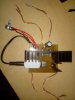
1
You have your Power supply electrolytic at one side of the board and its companion HF/RF ceramic decoupling capacitor at the complete opposite side of the board with all of that inductive foil path between them.
2
Move the units to the YELLOW and RED circle positions RIGHT up near the pwr chip.
3
Might as well move the decoupling capacitors associated with the 3 terminal regulator right up beside its terminals also. Consult the 3 term regulator data sheet as to the preferred and types of capacitors + values.
4
With your choosing of BTL mode your mind must have been oriented to power output and at max power . . . . . that will be requiring one healthy size heatsink for cooling that small footprint PWR IC
and your choice seem adequate.
5
The YELLOW boxing is relevant to what looks like a solder bridging, but was probably created in pulling the PWR IC and will later be corrected.
6
Do not see any capacitive isolation on each of your AUDIO inputs.
7
Your chip failure could have been attributed to that long inductive foil path and its distant bypassing having that unit operating as a power ultrasonic <--------> RF oscillator.
SCALED AND MARKED UP REFERENCING . . . . .
73s de Edd