Maker Pro
Maker Pro

Is anyone familiar with this type of MOSFETs' gate driver circuit?

This mosfet driver is a part of a welder inverter.The transistor Q2x is strange to me, I don't know why they add the transistor in this position. I tried googling many times but found no answers. Could you please help me? Also, could you please give me reasons for adding R6x and C4x into the circuit?

PS: I'm not sure whether d3x and d2x are both zener diodes or not since their names disappear.

Thank you
BlackMelon
 

Attachments

  • DDRive.PNG
    DDRive.PNG
    28.5 KB · Views: 143
Last edited:

(*steve*)

¡sǝpodᴉʇuɐ ǝɥʇ ɹɐǝɥd
Moderator
it seems to me that the circuit prevents the mosfet from being turned on for too long.

I have not done much analysis, but it seems that the top bjt is turned on a short time after the gate drive is applied to the mosfet, this turning the most off.

perhaps it limited the duty cycle? The gate resistors are such that it doesn't look like turn on speed is important.
 
I've just updated the circuit attached to the first thread to make it easier (just rewire wires) and it's something like a multistage amplifier.
However, voltage driving these BJTs' base pins is DC voltage so I don't know how they switch the power MOSFET on and off.
 

(*steve*)

¡sǝpodᴉʇuɐ ǝɥʇ ɹɐǝɥd
Moderator
OK, redrawn, it now looks like an oscillator. I confused one of the connections as where the gate drive was coming from.
 
Ok, so here is a pdf file presenting a power schematic of the welder. I hope it will provide us some more information about how this oscillator works. Moreover, I still have another questions left (I used to crop an image of some unknown connections to search for their topologies on Google picture search, but I still can't find my answer).

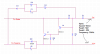
First, it starts from the "Board A". As a user hits a switch U15, 220 volt enters the board to reduce a common mode and differential mode noise. L3 and L4 are coupled inductors on the same ferrite core.
My question at this point:
1. Since C25, L3 and L4 can effectively annihilate a CM and DM noise, why they put C17,18 and 19 to do the same job twice?
2. When the U10 relay is NC, what do R35 and R36 do?

Second, we are now at the "Board B". It rectifies an AC signal.
1. However, what is the purpose of putting R37, R38 and the four capacitors paralled to them?

Third, at the board C, a 2 switch discontinuous mode flyback converter controls the amount of the welder's output voltage.
1. Why must they add components to the right of D11 and D6?
2. Could you please explain the gate driving sub-circuit? I've simulated buy putting a square wave to the node "Red2(S)-C". The result, as predicted, is just the wave-1.4V (1.4V from D2 and D4 voltage)

Fourth, at the board D, D15,16,17 rectify the welder's output current. Also, they put D18 and D14, acting as freewheeling diodes, which provide path current from the welder's load and inductors in the case that D15, 16, and 17 are turned off. C13, R30, C12 and R29 are acting as a band-pass filter.
My question:
1. Since the welder is a dc-output type welder, why do we need a band-pass filter? Are D17, 16, and 15 enough to provide dc current?


Board E:
Almost unknown about these board. Seems like a feedback system and protection system.

Board F:
It receives a signal from a signal board at Yellow(s)-F and Yellow1(S)-F and rectifies it into dc. This dc passes through an oscillator, as mentioned by steve, the output of this board, A1-A2, is sent to a transformer near board D
My questions:
1. Is this a technique for decreasing or limiting the welder's output current? (My reason is that since voltage across A1 and A2 can be controlled, we can control the amount of a TX4 secondary side voltage, allowing us to increase or the decrease amount of output voltage)
2. I do not quite familiar with this type of oscillator. Do you figure it out?
 

Attachments

  • Present.pdf
    68.5 KB · Views: 343

(*steve*)

¡sǝpodᴉʇuɐ ǝɥʇ ɹɐǝɥd
Moderator
You can't "annihilate" noise, just attenuate it somewhat. The additional components are probably just part of the network that does this.

R35 and R36 reduce the surge current when the unit is switched on. They allow the filter capacitors to charge slowly.

R37 and R38 are there to discharge the capacitors when you turn the power off. They also might have a limited function in ensuring the capacitors have the same voltage across them.

C20 to C23 are the main filter capacitors for the approx 400VDC supply.

Black(s)-E and Red(s)-E on board E are where the open circuit voltage is sensed. The hall effect sensor senses the current. BOard E is a snubber network for the output and probably part of the overvoltage protection network.

The output of Tx5 us rectified (half wave) and this pumps energy into L2 via the load. During the time when these pulses are not pumping energy in, the energy is released into the load via the flyback diodes. This operates in a similar manner to switchmode power supplies. C11 & C12, R29 & R30 are more snubber networks to protect the diodes.

The components to the right of D11 and D6 are snubber networks to protect the mosfets from voltage spikes.

Board F is the oscillator which drives the flyback inverter and is probably gated by the voltage and current limits.

The oscillator is simply an astable multivibrator. It's just not drawn the the traditional way.
 
Thank you, that helps me much. Still, I have something in my mind left.
1. Can we change C20-C23 and R37,38 into just an R in parallel with a C?
2. About snubber networks in board C, for R21,20 and C7, I can understand because its group is connected across drain and source of M6. However, do you mean that C6, R15,16,17 act as a snubber also? If so, what device do they protect?
 

(*steve*)

¡sǝpodᴉʇuɐ ǝɥʇ ɹɐǝɥd
Moderator
c20 to 23 are not a snubber network. They filter the pulsed output of the rectifier into dc.

ill look at the others later. I'm about to spend 7 hours driving a medic around.
 
Steve, what a gate driver circuit is it in board C? This technique is pretty strange. The two input wires are white2(S)-C and red2(S)-C. The output is connected to gg and S nodes of power MOSFET.
 

(*steve*)

¡sǝpodᴉʇuɐ ǝɥʇ ɹɐǝɥd
Moderator
White is the +ve supply, S is gnd.

Red is the signal input, and gg is the drive to the gates.

The circuit is kinda weird. Is it possible you have a few components incorrectly drawn?
 
I'm pretty sure that what I just posted is actually in the board because I checked 10 times. After your warning, I just rechecked it again...

However, there is a possibility that my customer took this broken-down welder to another repair shop before. That shop might just tamper with the device or attempt to replace burnt parts, but finally, he couldn't get it worked. As a result, a weird circuit was constructed.

Luckily, I found something interesting!. From the attached picture, I've just measured the signal between red and white, making me know the signal was just merely a bipolar driving signal! I guess this signal is just buffered or amplified to gate-source (since the presented circuit can't get the inverter board worked and heat some parts up, I can't conclude yet about what a correct gate-source signal is)

Is there any circuit that is close to this wrong one but produces any sense?

Thank you
 

Attachments

  • Red-White.jpg
    Red-White.jpg
    45.2 KB · Views: 68

(*steve*)

¡sǝpodᴉʇuɐ ǝɥʇ ɹɐǝɥd
Moderator
Finally we get some useful information! You have a unit with a fault, not some idle curiosity about the circuit!

What would be ideal is a picture of the board with the components that get hot (please point them out and indicate which ones they are on your circuit). Please give us a photo of both sides of the board in sufficient detail so we can read any markings on the board and components. Also, a photo of any board with damaged components.

Then...

What would be interesting is to look at the three points red, gg, and white with respect to S.

I expect white/S to be either DC, or similar. (make sure you use DC coupling)

I expect white/gg to be a similar signal to white/red, but possibly inverted (which makes the circuit diagram wrong) .

Do you have a dual trace scope? can you show both red and gg simultaneously wrt S.

And finally a caution. What sort of scope are you using? Are you sure that no part of the circuit is ground referenced? If it is, it is dangerous to you, your scope, and the device to connect the ground lead willy nilly to the circuit.

Just checking the diagram again, you have drawn both red(s)-E and white(s)-E as being connected to the same point on board E, and to what appears to be the power supply as well as the signal on board C. It is possible that I have been confused by the way you've drawn the circuit (as I was initially for q2x/q3x on board F).

We may have to start from (almost) scratch, verifying the presumed operation of each part of the circuit...
 
I'm sorry that I forget to tell you this before: Red(S)-C and Red(S)-E are not connected to each other. Their meaning are just "a red signal wire on a board C" and "a red signal wire on a board E" respectively. This rule is applied to other signal wires. However, all signal wires are connected to a signal board with different connectors. The waveform above actually comes from a signal board, and is voltage across White2(S)-C and Red2(S)-C.

Here is the photo of the board: https://www.mediafire.com/?c3yw7666bhv6s9o
From the schematic previously posted, the group R1-R5-M5 is paralleled 4 times. (Just simply parallel for higher current rating) You can notice this in a board by looking at the file Top_Overview_Colored. The unnamed resistors represent resistors in the group. The TVS diode U2 and U1 in the schematic just represents only 1 part. In Top_Overview_Colored file, the D13 and C2 have problems. the diode is toasted and the cap heats up. The rest of the files is just zooming parts and small areas, which might not be able to be seen in the Overview. I've also provided the bottom side of the board for you.

For measuring signals, I'll do it ASAP tomorrow cuz it's late night here.

Thank you
 
Last edited:
According to the previous discussion, the zener and capacitor having problems is desoldered.

https://www.mediafire.com/?89nyx8uxs51i00w
Here, I've got signals of Red and White with respect to a MOSFET's source (S). For a scope settings, I checked that my ground levels of both channels were set at Y=0 on displaying screen, and signals are measured in DC coupling mode. The signals swing below 0V.
The yellow trace = Red wire
The blue trace = White wire


https://www.mediafire.com/?53vf2r75x15s9qc
What's more, this is a video showing gg and a MOSFET's gate signals respected to a MOSFET's source (S).
The yellow trace=gate
The blue trace = gg

Thank you
 

(*steve*)

¡sǝpodᴉʇuɐ ǝɥʇ ɹɐǝɥd
Moderator
I'll take a look at this stuff later, but I had assumed the circuit shown was complete and the various wires connected between boards.

Can you get a schematic of this signal board too?
 
Top