Maker Pro
Maker Pro

Interfacing hall-effect sensor to embedded CPU

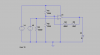
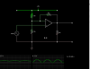
I'm trying to interface an Allegro A1160 half-effect sensor to a TI MSP430 CPU.

The A1160 is a 5V device whilst the MSP430 operates from a 1.8V to 3.6V supply. The MSP430 has onboard ADC, but the analog input pins have an absolute max rating of VCC + 0.3V.

I have both 3.3V and 5V regulators on my PCB design and I'm assuming that I'll need some opamps or something to interface between the MSP430 CPU and the A1160 sensor.

I'm still fairly new to electronics design and I'm looking for advice as to a good way to interface these two devices.
 
Hi Stube
I went to the Allegro site but found that they don't list an A1160 sensor. Would you please check the designation of the component?
Thanks!
 
Thanks Stube40
According to the Allegro datasheet, the chips have a "clamped low impedance" output. It sounds like all you need is a resistive potential divider.
:)

rethink...
The output voltage of the device will depend on the magnetic field. There's not much current available, so your ADC is probably safe, but perhaps it's a good idea to put a zener diode across the i/p of the ADC to be safe.
Once you know the likely voltage swing due to applied magnetic field you'll be in a better position to decide how to condition the signal for the ADC input.
You could measure this swing with a meter or oscilloscope, and write back to the forum for further advice.
 
Last edited:
Thanks Stube40
According to the Allegro datasheet, the chips have a "clamped low impedance" output. It sounds like all you need is a resistive potential divider.
:)

rethink...
The output voltage of the device will depend on the magnetic field. There's not much current available, so your ADC is probably safe, but perhaps it's a good idea to put a zener diode across the i/p of the ADC to be safe.
Once you know the likely voltage swing due to applied magnetic field you'll be in a better position to decide how to condition the signal for the ADC input.
You could measure this swing with a meter or oscilloscope, and write back to the forum for further advice.

Thanks poor mystic,

I have managed to acertain that the magnetic field I will be measuring should not exceed 200 Gauss, and is more likely to max out at 50G during normal operation. Hence, with the A1360 this means a maximum output of less than 300mV and a normal operating range of 0 - 60mV - this is without taking into account any DC offset that the device might have and doesn't consider if the device will have negative output depending on the polarity of the magnetic field (which I think it might).

I'm still trying to come to terms with the "user-adjustable quiescent voltage" in the data sheet that may be related to this.

Eitherway, it looks like I'm going to need some amplification.

I suppose my utopian scenario would be for the CPUs ADC to receive a signal that defaults to 1.5V for 0G, then goes to 3.0V for 200G and down to 0V for -200G.
 
Hi Stube40
I don't really think that i am the best person using this forum to advise you exactly how to go about your project from here... I knew this from my first post but I also knew that whoever the best person really is they would need the information I asked for.
Let's hang in for a bit and see if someone with more developed interfacing skills offers you some help.

I'll just use this last paragraph to put in a plug for "The Art of Electronics", a book by Horowitz and Hill which contains information I think you'll need.
Cheers! I'll look in later and see how it's going.

Mark
 
Thanks Mark. Appreciate your time. Will have a stab at it myself and see what I come up with then report back to this thread, at which point I'll either get a massive pat on the back or I'll have to hang my head in shame as my design is shot down in flames.

Either way, it should be a good learning experience for me!!
 
... I notice that the device wants a fairly high resistance in the output, at least 4k7. Also the datasheet says that an absloute maximum of 3mA current can be supplied by the o/p.
Therefore I suggest that if you do use a resistive potential divider you might want a total resistance of about 10kOhms, perhaps made up of a lower resistance of 6k8 and upper resistance of 3k3.
You might want to trim one of the resistors with a suitable potentiometer (a 10 turn pcb pot sounds good to me) so that you make the best use of the output by seeing to it that the maximum voltage that the sensor can provide is just a little lower than the the maximum that gives you a meaningful reading on the ADC.
 
Yes, you can use a resistive divider (pot) on the output as suggested by p.m.
I'd figure you can also put a variable resistor on the filter pin to pull down the voltage, but I don't know what temp.coeff. the internal resistor has - thus affecting accuracy.
I figure one won't need to adjust the internal quiescent voltage (2V), that would be better to calibrate in software. Notice the output won't go all the way to the supply rails.

Thanks Resqueline for joining in.

I've been studying Horrowitz and Hill (thanks Mark).

The A1360's quiescent voltage is programmable, but by default is 2.0V (approx 50%??). This is probably a good level to leave it at if I want to support bi-directional operation for measuring both negative and positive mag fields (which I do).

I've established that the biggest mag field I'm going to need to measure is 200 Gauss, which equates to a 280mV in either direction from the 2.0V.

Hence, I really need some amplification. Now the confusing part - how do I amplify with a 2.0V offset? I probably need about 6x amplification to turn the 280mV swing into a 1.68V swing. However, I don't want to multiply the 2.0V offset by 6x and end up putting 12V into the ADC when there is no field.

All I can think off is to set the quiescent voltage to zero and then amplify, but then I will only have unidirectional measurement capability.
 
Good Morning Stube40 :)
the amplification setting of the attached circuit relies partly on the Thevenin equivalent resistance of the voltage divider at the inverting input, and partly as usual on the feedback from o/p to the same inverting input. The o/p swings about the divider voltage at an amplification trimmed by the 2kOhm 10 turn pcb trimpot. The o/p is limited by a zener diode to a maximum of 3V.
 

Attachments

  • edited output.jpg
    edited output.jpg
    18.1 KB · Views: 684
darn it, I have drawn the resistors the wrong way around... the 3k3 and the 2k2 are in each other's places

Hi Mark,

Thanks for all your time. I've spent the morning learning how to use LTSpiceIV (was amazed that LT give it away for free on their website!!!). I used it to simulate the circuit you posted as shown in the attached picture. I kept the variable resistor at 1k for the moment.

I put two voltage sources in - one to represent 5V Vcc and the other to represent the output from the sensor - in this case a 50Hz sine wave with 1V amplitude centred around 2V.

I've attached a picture which shows what happens when I run the simulation - the output appears zero (V_n003) and when I zoom into it (zoomed picture attached) I can see that there is some distorted version of the sine wave but at a tiny amplitude.

I don't think this is what we expected to see, but possibly it's because my simulation is not right?
 

Attachments

  • Circuit.PNG
    Circuit.PNG
    20.4 KB · Views: 1,055
  • Simulation Outputs.PNG
    Simulation Outputs.PNG
    23.8 KB · Views: 192
  • Output Voltage Zoomed.PNG
    Output Voltage Zoomed.PNG
    39.8 KB · Views: 210
Well Stube40 :)
Thank you very much for your latest post. As for the results of the simulation, they sure ain't what I had expected to see.
This is the kind of time I am grateful that there are several much more experienced men than myself contributing to the forum.
 
The screenshots needs some additional information:
green = node 4 = V2 = 2V +/-0.5V = non-inverting input
red = node 2 = 2.6V = inverting input?
cyan = node 3 = 0V = output
blue = node 1 = V1 = 5V psu
Of course, with the 3.3k to ground there will be 3V on the inverting input, not 2V as intended - and as was shown correct in p.m.'s initial diagram.
 
Hi again Stube
I checked the circuit using the circuit simulator at http://www.falstad.com/circuit/ and when I gave the input 2VDC+300mVAC at the input, with the 5V rail, I got the results shown in the attachment.

Still, I feel there are better ways to go about obtaining your measurements. I believe that it may be better to interface as directly as possible to the ADC in this case. This is partly because you would otherwise wish to change the range of the measurement, which I think you'd be better off doing in software, and partly because of reliability issues.

I feel that the first step in this desgn project should have been a noise specification. You need to say exactly what resolution you want and at what sample rate, et cetera. Then you have a rational basis for the choice of an ADC and sampling methods.
Say you need 16 bits of accuracy in your measurement of the magnetic field. That is to say that the 300mV range needs to be 16 bits. Add 4 more bits to cover the rest of the range of voltages through which the input will move (because the range of the ADC is more than 8 times the range of the signal of interest), and you find you need at least 20 bits of resoution in your ADC.
I googled for 20 bit ADC's and found that they are in plentiful supply.
 

Attachments

  • Hall Effect.png
    Hall Effect.png
    14.8 KB · Views: 355
Hi guys - thanks once again for all the help.

PM - I'm going to have a try of that Falstad simulator you've used and take it from there. Will be interesting to see if I can get the same results as you (in other words - to see if I can use the SW properly). Thanks for the tip. Also, 20-bit ADC could be the way - there's plenty with either SPI or parallel interfaces.

Will report back soon. Thanks.
 
Good on ya Stube40
... there are ADC's with all kinds of resolutions - you can get 64 bit devices quite readily. That's why I say that your carefully defined needs should drive your choice of interfacing equipment.
;-)
 
Hi PM,

The Falstad circuit simulator is a lovely little tool - so straightforward and a great UI.

Everything was going well until I started making my own circuit and keep getting bad connections (ie the node "dot" goes red instead of being white and I get a "bad connection" text sign).

Can't quite work this out - I re-drew some of the circuit and the bad connections went away, but other parts of the circuit just can't seem to be put together without a bad connection. Weird. I'm assuming that the problem is me, since this would make it very unpopular if everyone had the same experience.

Can you shed any light on it? The instructions are fairly sparse.........
 
Top