Maker Pro
Maker Pro

Interesting wiring in designing an evaluation board for a capacitive readout sensor

Hi,

Please allow me to describe my situation first.I recently bought a capacitve readout sensor from a small Japanese company. Although this product is no longer manufactured several years ago, the company still has some inventory, so I could get some chip, but no evaluation board and no technical people answering my question when I try to build my own evaluation board.

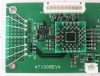
What I have now is the evaluation board circuit diagram and a blurry picture of real object I got from the manual, as shown below.

This readout sensor has three channels X,Y,Z, each channel can measure the difference between two external capacitors,for example Cx1-Cx2. The capacitors share one common electrode which is directly connected to pin SI on the chip.

There is a buffer(see the red arrow) which is used to reduce noise.
From the circuit diagram we can see
1.the non-inverting input is connected to SI;
2. inverting input and output are connected together
3. the connected inverting input and output are separated later.

My question where should I connect the separated inverting input and output to?

I am trying to answer this question by comparing the diagram with the real object. But I found something confusing.
1.The SI pin in the picture of the real object(red arrow)seems isolated from the SI port on the port.
2.I think the two holes on top of and at the bottom of the SI pin should be the inverting input and output in the circuit diagram, but what's the point of making such wiring.


upload_2015-12-11_16-16-11.png

upload_2015-12-11_16-34-27.png
 

Attachments

  • upload_2015-12-11_16-17-28.png
    upload_2015-12-11_16-17-28.png
    473.7 KB · Views: 71
It is very hard to get to get to any conclusion from the board photo,
because this may very well be a multiplayer board.
and the piggy-back board blocks the view of the traces on the photo.

The op-amp connections are clearly an optional one on the evaluation board.
The number 1 and 2 pins of the op- amp are the yellow traces.
The number 3 pin of the op-amp goes to a via and from there ?

To answer your question a datasheet of the AT1006 IC is needed,can you post it?
Is SI an output?
if so maybe that is the purpose of this kind of connection-to allow the capacitors to be connected either to the SI directly or to it buffered.

piggy.jpg
 
It is very hard to get to get to any conclusion from the board photo,
because this may very well be a multiplayer board.
and the piggy-back board blocks the view of the traces on the photo.

The op-amp connections are clearly an optional one on the evaluation board.
The number 1 and 2 pins of the op- amp are the yellow traces.
The number 3 pin of the op-amp goes to a via and from there ?

To answer your question a datasheet of the AT1006 IC is needed,can you post it?
Is SI an output?
if so maybe that is the purpose of this kind of connection-to allow the capacitors to be connected either to the SI directly or to it buffered.

View attachment 23679
Thanks for your reply. The manual is in Janpanese, I am not sure if it will help. The manual can be found at http://www.actlsi.co.jp/pdf/at1006_manual.pdf, it's too large to be attached.

SI is the common point of two capacitors, it actually is connected to another op amp's non-inverting input inside the chip (different om amp from the one we mentioned above). This is related to the working principle of the the differential capacitive readout sensor, it is actually a charge amplifier like shown below.
upload_2015-12-11_17-31-48.png
Periodic out of phase square wave are applied to C1 and C2 by controlling the switches. If doing this the output voltage is proportional to C1-C2, from which we can obtain the capacitance difference.
 
From the Datasheet block diagram(pp.13) it is clear that SI (Sensor- Input ?) is an input.
It is pin 8(pp.45),therefor what you marked as SI in red isn't SI.
I assume that SI is buffered by the op-AMP for off-board optional use.

I don't know why the yellow lines go towards the AT1006 IC.

piggy-1.JPG
 
From the Datasheet block diagram(pp.13) it is clear that SI (Sensor- Input ?) is an input.
It is pin 8(pp.45),therefor what you marked as SI in red isn't SI.
I assume that SI is buffered by the op-AMP for off-board optional use.

I don't know why the yellow lines go towards the AT1006 IC.

View attachment 23681
I think you are right, SI is an input. But the point I marked is SI, I am pretty sure about that. I am sorry I should mention that the pinout connection you see in the manual is for PGA64 package, while the evaluation board circuit diagram is for LQFP48 package which is also the package type of the real chip object I got. The evaluation board in the picture should be accompanied with the LQFP48 package, but somehow they replace the LQFP48 chip with the PGA64 while remaining other parts unchanged. That's why you see the piggy-back which seems not compatible with the other parts of the evaluation board.

I suspect that the central hole where the arrow points to is not totally isolated as it seems to be. It might have some openings, like upload_2015-12-12_10-19-10.png, the signal is still connected to the surrounding area. In this case the three holes should have the same voltage, which agrees with the circuit diagram from which we can see the non-inverting and inverting input and output have the same voltage.
 
"In this case the three holes should have the same voltage, which agrees with the circuit diagram from which we can see the non-inverting and inverting input and output have the same voltage."

I don't see any connections like that,only pins 1 and 2 of the op.amp are connected together in the diagram.
Furthermore, It makes no sense connecting pin 3 to 1 and 2 that would be a meaningless circuit.
I would suggest you either omit the op. amp from what you build or connect it as an option with pins 1and 2 connected to SI and pin 3 being a buffered version of SI for whatever application that needs that.
See pages 13 and 14,no op.amp required.

BTW,
How would you write the software for interfacing this IC,can you read Japanese ?

upload_2015-12-11_16-16-11.png
 
"In this case the three holes should have the same voltage, which agrees with the circuit diagram from which we can see the non-inverting and inverting input and output have the same voltage."

I don't see any connections like that,only pins 1 and 2 of the op.amp are connected together in the diagram.
Furthermore, It makes no sense connecting pin 3 to 1 and 2 that would be a meaningless circuit.
I would suggest you either omit the op. amp from what you build or connect it as an option with pins 1and 2 connected to SI and pin 3 being a buffered version of SI for whatever application that needs that.
See pages 13 and 14,no op.amp required.

BTW,
How would you write the software for interfacing this IC,can you read Japanese ?

View attachment 23684
Thanks for your reply.

Pin 1(op amp output) and pin 2(inverting input) are connected together which have the same voltage. Typically I think we can consider pin 2(inverting input) and pin 3(non-inverting input) have the same voltage for an op amp. That's why I said the three pins have same voltage.

I learn about this chip from a paper written by a Japanese professor. He gave me a labview program which can be used to control registers in the chip.

The op amp is necessary because it can reduce noise as mentioned by that professor. The chip measured very tiny capacitance difference. Reducing noise is of vital importance.
 
Top