Maker Pro
Maker Pro

How is current passing through the capacitor in the following schematic?

Question derived from experiment 11 from Make:Electronics 2nd edition by Charles Platt.

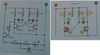
The author explains that when Q1's base is positively biased, Q1 begins sinking current from the left side of C1. Also the right side of C1 goes momentarily below zero volts.

My thought is that current can only sink from the left side of C1 if the right side of C1 has a path back to the left side of C1. Assuming this is true, the right side of C1 must be traveling through Q2; however, since the base of Q2, a NPN transistor, is negatively biased Q2 is "closed" not allowing the path to complete back to the left side of C1.

So how is the capacitor passing current through Q1? What assumption am I making that is incorrect? Any help would be greatly appreciated.
 

Attachments

  • make11.png
    make11.png
    448.5 KB · Views: 21
Current does not "pass through" a capacitor. Instead a capacitor charges or discharges.
A transistor is not open or closed like a door. Instead a transistor is turned on or is turned off.

If Q1 is turned off and Q2 is turned on then C1 is charged by r1 and the base-emitter diode of Q2.
The left terminal of C1 is near the positive supply voltage and the right terminal is at about +0.7V.
Then when Q1 turns on the left terminal of C1 goes to almost 0V and the charged voltage of the capacitor drives the right terminal to a negative voltage which turns off Q2 and C1 discharges into R1.
 
It is the capacitor discharging that is confusing me in the schematic. The capacitor will not discharge unless the capacitor has a complete path correct? For example, I have attached a drawing. Let's assume that the capacitor is charged and inserted into the schematic. If I pull the power source the capacitor will not discharge because the right side of the capacitor does not have a path back to the left side of the capacitor. How is the path completed for C1? I don't believe that Q2 is providing the path is it? Am I wrong in this assumption? Even though Q2 is off, it still provides a path back to C1?
 

Attachments

  • make11_2.png
    make11_2.png
    2.9 KB · Views: 4
Your diagram #3 is not complete but if you refer to the original you will see transistor junctions that allow certain current flows.
 
Your diagram #3 is not complete but if you refer to the original you will see transistor junctions that allow certain current flows.
Yes, I was trying to convey in diagram #3 that a complete path is necessary for the capacitor to discharge. In the original schematic, I didn't believe that the path was complete because the transistor Q2 was off and therefore not completing the path similar to diagram #3. I don't see how Q2 is completing the path since it is off. I am going to try some experiments with running the capacitor through a transistor and see if it in fact does complete the circuit.
 

davenn

Moderator
@prestonElectronics
welcome to EP :)

As Audioguru said, current doesnt pass through a capacitor
See the symbol for a capacitor ?

cap.jpg

there's a gap in the middle, between the two plates, so nothing "flows" across that gap
As, say, the left plate energises, goes more negative, as charges (electrons) flow into it.
An equal number of charges (electrons) leave the right plate. This gives the impression
of current flowing through the capacitor
 
I already explained how the capacitor C1 is discharged:
"Then when Q1 turns on, the left terminal of C1 goes to almost 0V and the charged voltage of the capacitor drives the right terminal to a negative voltage which turns off Q2 and C1 discharges into R1."
 
The "cookbook" shows the circuit using a 9V supply and does not say that the capacitor driving the base of the transistor to almost -9V damages the transistor since its absolute maximum allowed reverse emitter-base voltage is only 6V.
 

Attachments

  • multivibrator voltage problem.png
    multivibrator voltage problem.png
    47.7 KB · Views: 6
Below is the LTspice simulation the circuit, to perhaps help clarify what has been said:

The Q1 collector voltage (yellow trace) shows the waveform driving C1.

The red trace shows the capacitor C1 current, which has a small, longer current pulse when Q1 goes high, and a higher, shorter current spike when Q1 goes back low.

The white trace shows the voltage across C1 (Q1 side is positive).

The green trace shows the current through R3, which is charging the capacitor when Q1 goes low.

The blue trace shows the current through Q2's base from the capacitor, which turns it on when Q1 goes high.
The negative current spike is from the base-emitter junction capacitance).

The purple trace shows the Q2's base voltage going to -9V (with a 9V supply), which will likely damage it as AG noted.

upload_2022-2-6_14-9-15.png
 
I appreciate all the responses and apologies for my sloppy title which I think threw off some of the responses I received. I still need to do some experiments on the breadboard to get my head around this but wanted to get on here to thank all of you.
 
Top