Maker Pro
Maker Pro

Help repairing Samsung VHS/DVD Combo - No power

Greetings! I am new to the forums and hopeful that someone can assist me in repairing a couple of old VCR's.
The first VHS/VCR is a Samsung DVD-V4600 unit I purchased at a thrift store. I happily brought it home and plugged it in to find that it had no power whatsoever. No lights, no blips, nadda. Dead. Now I'm not so happy. I unplugged the unit, took off the lid and did a visual inspection. The unit, to my surprise, looks pretty clean. I examined the components and I do not see any visual indicators as to the issue. No bulging or leaky capacitors, no burn marks, etc. The fuse is not blown. I plugged the unit in and noticed a buzzing/humming noise coming from the power supply area. (Naturally I googled "buzzing smps" thinking this would lead me in the right direction. Sadly, unlike on television, google was utterly useless). Determined not to give up I spent hours googling and reading about switch mode power supplies. I bought a capacitance meter and discharged the big main capacitor and measured it. It seems fine. I then tested what I believe to be the "startup" resistors. I removed one leg from the board first. These measured fine also. Next I considered testing the mosfet but the transformer is blocking my screwdriver making it difficult to remove. I'm hoping someone can give me advice on what to try next... Photos of the power supply are below (I've indicated the capacitor and resistors I tested in the second photo). Any questions please let me know and thank you in advance for any help you can provide!

Summary:
No visual signs of defects (bulging, leaking capacitors, etc.)
Buzzing noise coming from power supply
Tested large capacitor and startup resistors = ok
Fuse is not blown

I was able to find the service manual online. Here

1VCR.jpg

1VCR-B.jpg
 
I'm no expert, but I'll warn you that a Smps can be very difficult to repair due to their complexity.
Also beware that dangerous high voltages are present that can knock you on your arse (or worse).

I'd start by checking diodes and mosfets.

You may want to pull out a component in series with the ps incase there is a downstream short dragging voltage down. Then put a light resistive load across (parallel) the power supply sized less than the ps rating. This will isolate wither its the ps or something downstream shorting it out.

If ps voltage doesn't come up, opto isolator, transformers, or the ic controller could be bad.

I can remove one leg of each diode from circuit and test them all. Should I do this for all the capacitors and resistors as well? (I do drain the capacitors with a resistor before de-soldering for safety.)
I'm fairly new to electronics so I'm afraid I am not entirely sure how to perform the above quoted advice as far as picking a component to pull and how to safely apply lighter power to the circuit.

Thank you for your help so far. It's appreciated.
 
I can remove one leg of each diode from circuit and test them all. Should I do this for all the capacitors and resistors as well?.
Yes, it's a good idea in order to get a reliable reading although cap ESR testing can be done in circuit.

Ceramic disc caps don't fail very often if they look ok, so I wouldn't bother checking them at this point.

Btw, welcome to the forum WyluliWolf
 
The 'buzzing' tells me that the supply is constantly cycling through boot-up - and failing due to a problem on the SECONDARY side.

If you can remove the PSU as a module and test it with just an AC mains input (appropriate precautions to be taken of course) you might find it boots properly and you'd then be looking for problems elsewhere in the unit.

Although bulging capacitors are a decent sign of problems they don't always afford us the convenience of 'bulging' to make fault finding easy. You would HAVE to test them to prove their legitimacy.

Such testing would have to be done out of circuit - they frequently parallel capacitors on the low voltage side so in-circuit testing won't work.
 
The 'buzzing' tells me that the supply is constantly cycling through boot-up - and failing due to a problem on the SECONDARY side.

If you can remove the PSU as a module and test it with just an AC mains input (appropriate precautions to be taken of course) you might find it boots properly and you'd then be looking for problems elsewhere in the unit.
I was able to pull out the power supply board. I plugged it in and the buzzing/humming noise is still there.
I'll do some testing of the individual parts today. The schematic is included in the service manual (linked to above). Is there any other way to narrow down the testing or should I basically remove and test every component possible (sounds fun!) ;) There are quite a few electrolytic capacitors and even more diodes etc.
Thanks again!
 
I was finally able to get the MOS transistor out of the circuit for testing. I'm a little confused when trying to test this. I tried testing using my multi-meter using hfe (see photo). I believe I have it placed correctly (NPN and legs in the correct order of BCE) but please double check, I have been known to make mistakes. I seem to get no reading other than an occasional - sign. I then poked at it with the multi-meter in diode/continuity mode. You can see the results in this 17 second video. VIDEO
I also decided to pull one leg of one of the zener diodes. The test on that, in Diode mode, seems to indicate a bad part. I get a low reading in both directions. See the attached photo's.
transistortest.jpg zener1.jpg zener2.jpg

Is the transistor bad, or am I doing something incorrectly?
Is the diode bad, as I suspect, and in need of replacing?
What should I check next now that we have this info?

Thanks again.
 
You can't test a MOSFET in a standard transistor socket.....

The zener diode check looks to be dodgy - assuming the meter is being used correctly (have you checked the user manual for the correct operation of that mode?)

You can use the diode check mode to test the MOSFET - check between all lead combinations of the MOSFET and report back with the results.
 
Ok, good to know. The transistor/mosfet thing was a little confusing.
Photos with test results shown. (Note mosfet is face down).

MOSFET-Test1.jpgMOSFET-Test2.jpgMOSFET-Test3.jpgMOSFET-Test4.jpg

Positive lead to the left leg and center leg = no reading on either of the other two pins.
 
Last edited:
What is the actual part number on that 'transistor'?

I believe the service manual refers to this PART (The link to the service manual is in my first post in case that helps. It contains schematics and part numbers for everything). Attached is a photo of the front of the mosfet so you can see all the numbers.
Mosfet-Front.jpg
 
Sir WyluliWolf . . . . . .

I think what you may have yourself, there, is being a " soft " failure.
Should it have been a HARD failure, fully expect a blown line fuse-Rectifiers- and that Power transistor.
The final fault analysis should probably reveal either a time evolved onset of "atrophy " of one or some E-caps
in the unit.
Or . . . . there could be a shorted or high leakage of one or more of the diodes that rectify each of the secondary transformer windings to create their specific voltage supply output.
Or . . . there could be an atrophied / weak E-cap (s) on one or more of those secondary supplies.

Procedure: . . . . .

I believe that your zener is OK and you are actually reading the inits common junction voltage of 700mv, by virtue of the MANNER of its polarity, in which you are now testing it, wherein you are also not reaching the zener threshold with your test voltage level.

Put the PS all back together as it was and then refer to my marked up dupe of your photo.
I have dropped its contrast, to let otherwise obscured / darkened parts now being shown up visibly.

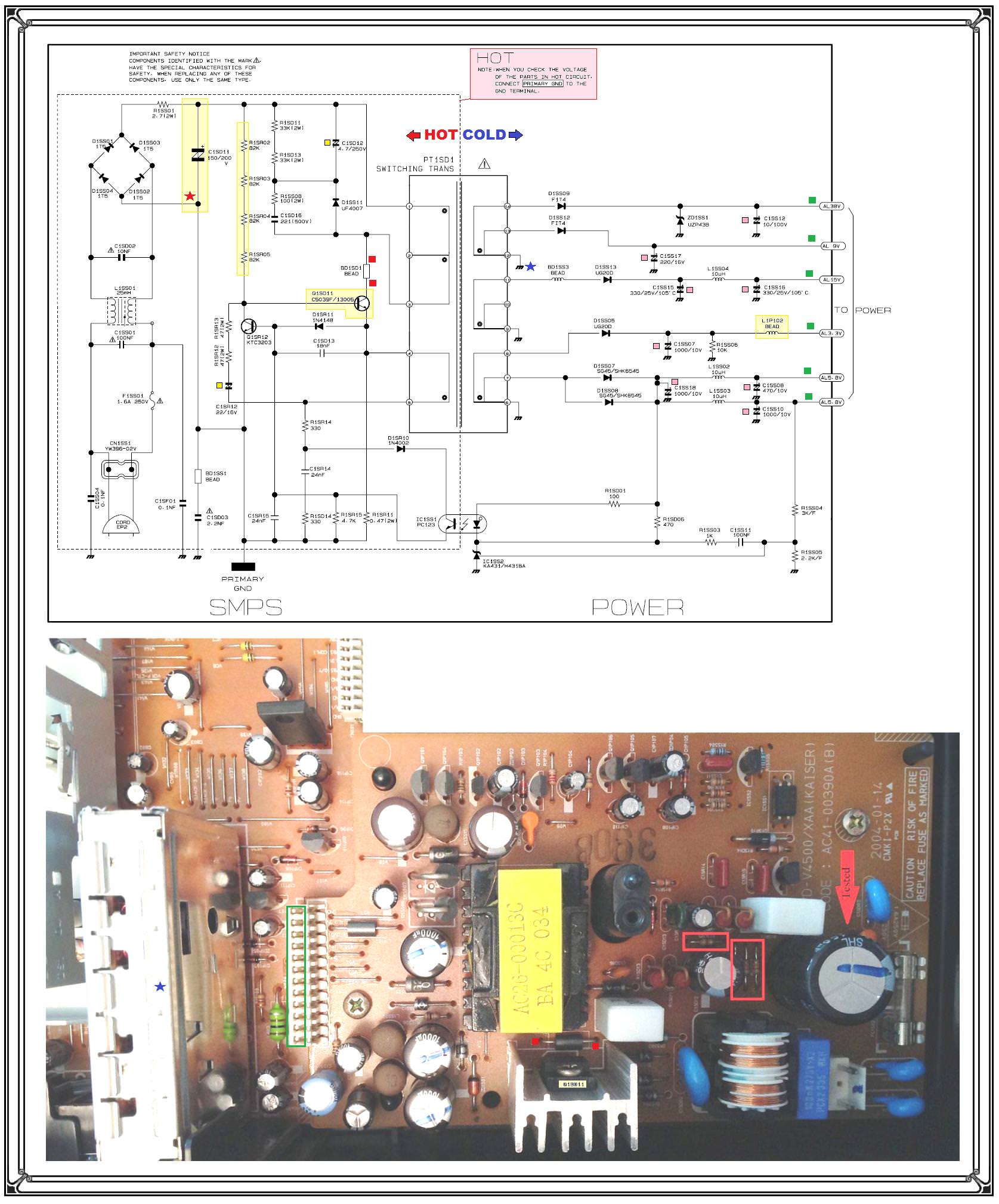
At the top schematic . . . . .points of interest, being . . . . The YELLOW C1SD11 is the main B+ electroltyic for the AC line derived HOT power supply.
The arrangement of a series of 82k resistors are done in that way, to physically string them out for voltage versus mechanical physical isolation considerations.
Their function is to initially supply a bit of start up bias to the Q1SD11 power osc transistor and Q1SR12 driver transistor AT THE INSTANT THAT YOU PLUG IN THE AC POWER LINE CORD.

ALL TIMES AFTER THAT . . . the power supply either runs at a standby reduced power mode or at full operational power mode when the unit is turned on at front panel or timer, or by remote control.
They would only come into play, if unplugged or having a line power disruption.

The only other immediate considerations on the LEFT half of the supply which is AC line POWER HOT, is the need to use the RED STAR ( or any of the 6 other direct part tie ins to it ) for any metered readings for your meters black ground lead.

Looking over to the BLUE . . .COLD . . . side of the supply, it is being isolated from the AC power line by the transformer.
Metering can use the BLUE STAR or any of the like symbols for negative meter lead.

The far right GREEN SQUARES are relating to different derived supply voltages . Moving to the left are the PINK E-caps related to filtering those different supply voltages.
Just to the capacitors left, would be the specific diodes which created those DC supply voltages .

HOW THIS SPECIFIC UNIT WORKS . . . .

With YOUR unit not having blown the 1.6 A fuse, just inline after AC line power input, we can run power up to the discrete 4 diode full wave bridge at the top left corner and derive DC voltage to charge up he YELLOW . . . .C1SD11S . . .MAIN E-cap and it then directs its stored power to the right thru the terms 1 & 3 top winding of the primary of the power transformer and then it passes to the left to the collector of Q1SD11.
The simultaneous voltage bump from the start up resistor string, keyed the base of the power transistor to create a pulse at the aforementioned primary winding. The then collapsing magnetic field from the primary , magnetically induces the secondary 4 &5 winding to create a voltage output pulse which feeds to base of Q1SR12 driver transistor. .
The collector of Q1SR12 then correspondingly, kicks out a drive pulse to the base of Q1SD11, so that it will then repeat that pulse output up at the collector.
Now you have yourself a self running power oscillator, but is being able to vary its output level by modification of the base drive of the Q1SR12 driver transistor.
That is being accomplished by the circuitry just below that transistor pair, which is being correctively fed by the varying output of the IC1SS1 , optical isolator, located just below the power transformer .
The use of an optical isolator also keeps the HOT AC Line operated circuitry at the left, electrically isolated form the safe low voltage secondaries on the cold side of the power supply.

Look to the right half of the IC1SS1 optical isolator and you will see that its internal LED is receiving a sampling of the +5.8VDC supply as is established by any turning on of the is sampling the IC1SS2 PRECISION REFERENCE ZENER
If the whole right half of cold supply voltages pull down under loading demands , the +5.8 supply also pulls down and varies the established brightness of the OI's internal LED , which alters the OI's other sides phototransistor to change the drive level to the power transistor to up its output to meet the altered power demands.
C1SR12 and adjunct resistances maintain a speed of response and recovery time , for stable compensatory power transitions .


HOWTODOITTOIT . . . . . .

HOT SIDE

Get DC metering set up between RED STAR ground and probe into the bare wire on either side of RED SQUARE sides of parasitic suppression ferrite bead at the front of Q1SD11 power transistor.
Be SURE that your probe pierces any clear lacquer coating that might be on the bare buss wires.
Then HOPE that your meters response time will let you make out some voltage peaks after you have plugged in and powered up the system. If you happen to have an old analog . . .needle . . .meter it would excel in this particular testing, vice a digital unit, since I see that your meter does not additionally, have any LCD hash mark "analog scaling"..

If you then detect any cyclic up and down voltage swings, one might consider the secondary "COLD" circuitry, and that a diode of a supply line might have dead shorted or its electrolytic that it supplies, might have DRASTICALLY reduced in capacitance with time.
This is particularly true of the + 5.8 VDC supply since it is used for feedback referencing of power control.

In metering the COLD supply, if you look at the marked up photo , it looks like you can see bare buss wires passing up to the WHITE connector I have marked with a GREEN RECTANGLE.
That would be easy access for meter probing with you using COLD ground meter referencing to the BLUE STAR of the metal housing to the left of the WHITE connector.
If you then DC meter those voltages, expect very low voltages that fluctuate in rhythm just like the HOT side voltage did.
The 26VDC supply would vary the most, and lower voltages , proportionately less, especially the 3.3..
If one does not vary at all, it might be due to its supply diode being shorted.
On the other situation, place your metering in AC mode and probe each supply, a high reading on a supply there would be indicative of a pooped capacitor that has lost its capacitance.

Now . . .go makee- testee-testee and feed back or initiate further querys.

MARKED ON PHOTO AND MARKED UP REFERENCE SCHEMATIC . . . . . .
B5j75wM.jpg


73's de Edd . . . . . .
 
Last edited:
Sir WyluliWolf . . . . . .

I think what you may have yourself, there, is being a " soft " failure.
Should it have been a HARD failure, fully expect a blown line fuse-Rectifiers- and that Power transistor.
The final fault analysis should probably reveal either a time evolved onset of "atrophy " of one or some E-caps
in the unit.
Or . . . . there could be a shorted or high leakage of one or more of the diodes that rectify each of the secondary transformer windings to create their specific voltage supply output.
Or . . . there could be an atrophied / weak E-cap (s) on one or more of those secondary supplies.

Procedure: . . . . .

I believe that your zener is OK and you are actually reading the inits common junction voltage of 700mv, by virtue of the MANNER of its polarity, in which you are now testing it, wherein you are also not reaching the zener threshold with your test voltage level.

Put the PS all back together as it was and then refer to my marked up dupe of your photo.
I have dropped its contrast, to let otherwise obscured / darkened parts now being shown up visibly.

At the top schematic . . . . .points of interest, being . . . . The YELLOW C1SD11 is the main B+ electroltyic for the AC line derived HOT power supply.
The arrangement of a series of 82k resistors are done in that way, to physically string them out for voltage versus mechanical physical isolation considerations.
Their function is to initially supply a bit of start up bias to the Q1SD11 power osc transistor and Q1SR12 driver transistor AT THE INSTANT THAT YOU PLUG IN THE AC POWER LINE CORD.

ALL TIMES AFTER THAT . . . the power supply either runs at a standby reduced power mode or at full operational power mode when the unit is turned on at front panel or timer, or by remote control.
They would only come into play, if unplugged or having a line power disruption.

The only other immediate considerations on the LEFT half of the supply which is AC line POWER HOT, is the need to use the RED STAR ( or any of the 6 other direct part tie ins to it ) for any metered readings for your meters black ground lead.

Looking over to the BLUE . . .COLD . . . side of the supply, it is being isolated from the AC power line by the transformer.
Metering can use the BLUE STAR or any of the like symbols for negative meter lead.

The far right GREEN SQUARES are relating to different derived supply voltages . Moving to the left are the PINK E-caps related to filtering those different supply voltages.
Just to the capacitors left, would be the specific diodes which created those DC supply voltages .

HOW THIS SPECIFIC UNIT WORKS . . . .

With YOUR unit not having blown the 1.6 A fuse, just inline after AC line power input, we can run power up to the discrete 4 diode full wave bridge at the top left corner and derive DC voltage to charge up he YELLOW . . . .C1SD11S . . .MAIN E-cap and it then directs its stored power to the right thru the terms 1 & 3 top winding of the primary of the power transformer and then it passes to the left to the collector of Q1SD11.
The simultaneous voltage bump from the start up resistor string, keyed the base of the power transistor to create a pulse at the aforementioned primary winding. The then collapsing magnetic field from the primary , magnetically induces the secondary 4 &5 winding to create a voltage output pulse which feeds to base of Q1SR12 driver transistor. .
The collector of Q1SR12 then correspondingly, kicks out a drive pulse to the base of Q1SD11, so that it will then repeat that pulse output up at the collector.
Now you have yourself a self running power oscillator, but is being able to vary its output level by modification of the base drive of the Q1SR12 driver transistor.
That is being accomplished by the circuitry just below that transistor pair, which is being correctively fed by the varying output of the IC1SS1 , optical isolator, located just below the power transformer .
The use of an optical isolator also keeps the HOT AC Line operated circuitry at the left, electrically isolated form the safe low voltage secondaries on the cold side of the power supply.

Look to the right half of the IC1SS1 optical isolator and you will see that its internal LED is receiving a sampling of the +5.8VDC supply as is established by any turning on of the is sampling the IC1SS2 PRECISION REFERENCE ZENER
If the whole right half of cold supply voltages pull down under loading demands , the +5.8 supply also pulls down and varies the established brightness of the OI's internal LED , which alters the OI's other sides phototransistor to change the drive level to the power transistor to up its output to meet the altered power demands.
C1SR12 and adjunct resistances maintain a speed of response and recovery time , for stable compensatory power transitions .


HOWTODOITTOIT . . . . . .

HOT SIDE

Get DC metering set up between RED STAR ground and probe into the bare wire on either side of RED SQUARE sides of parasitic suppression ferrite bead at the front of Q1SD11 power transistor.
Be SURE that your probe pierces any clear lacquer coating that might be on the bare buss wires.
Then HOPE that your meters response time will let you make out some voltage peaks after you have plugged in and powered up the system. If you happen to have an old analog . . .needle . . .meter it would excel in this particular testing, vice a digital unit, since I see that your meter does not additionally, have any LCD hash mark "analog scaling"..

If you then detect any cyclic up and down voltage swings, one might consider the secondary "COLD" circuitry, and that a diode of a supply line might have dead shorted or its electrolytic that it supplies, might have DRASTICALLY reduced in capacitance with time.
This is particularly true of the + 5.8 VDC supply since it is used for feedback referencing of power control.

In metering the COLD supply, if you look at the marked up photo , it looks like you can see bare buss wires passing up to the WHITE connector I have marked with a GREEN RECTANGLE.
That would be easy access for meter probing with you using COLD ground meter referencing to the BLUE STAR of the metal housing to the left of the WHITE connector.
If you then DC meter those voltages, expect very low voltages that fluctuate in rhythm just like the HOT side voltage did.
The 26VDC supply would vary the most, and lower voltages , proportionately less, especially the 3.3..
If one does not vary at all, it might be due to its supply diode being shorted.
On the other situation, place your metering in AC mode and probe each supply, a high reading on a supply there would be indicative of a pooped capacitor that has lost its capacitance.

Now . . .go makee- testee-testee and feed back or initiate further querys.

MARKED ON PHOTO AND MARKED UP REFERENCE SCHEMATIC . . . . . .
B5j75wM.jpg


73's de Edd . . . . . .
Thanks much for your reply. Give me a couple of days to digest this. I have a general idea on electronics but I have a lot more to learn so I may be a bit "slow" compared to the more seasoned veterans out there. I will report back.
 
I've read everything above but I'm not overly comfortable poking around a live power supply with my multimeter. I know the voltages are dangerous and my schematic reading skills are not exactly top notch. I don't want to make a potentially harmful or deadly mistake. I do appreciate the advice and if I were a more seasoned pro with proper safety equipment etc. I'm sure this would be a breeze.
I'm comfortable with testing diodes, resistors and capacitors so I may continue on that trail. I know it may not turn out to be any of those things but it's worth a shot.
I am a little confused with this statement:
"I believe that your zener is OK and you are actually reading the inits common junction voltage of 700mv, by virtue of the MANNER of its polarity, in which you are now testing it, wherein you are also not reaching the zener threshold with your test voltage level."
I pulled one leg of the diode from the circuit and tested in both directions with the diode setting on my multi-meter. The reading is the same in both directions leading me to believe the diode is no longer good. Were you assuming the diode was still in circuit when you made the above statement?

If i do replace the diode I notice that the part number doesn't seem to be listed in the service manual (just my luck). Location is ZD1SS1 and diode is marked with "Z43". Will a 4.3V zener diode such as this (1N4731A) work?
Reverse side of the board:
pcbbottom.jpg
 
Last edited:
Sir WyluliWolf . . . . . . ( not to be confused with Wily E. Coyote. )

To FULLY allay your fears and worries ingrained in your mind . . . ..about . . . " that zener diode".
It seems that zener diode is directly across the power supply section that is derived from the transformer winding terms 12--14 that feed diode D1SS09 for rectification . .. then your ZD1SS1is going directly to ground . . .IF and that's being very heaveeeeeee, on that IF, 43V is / will ever be experienced.
Since, that unit is a 43V zener diode and it serves a clipper of any overvoltage spikes on that supply, or it shorts , in the case of a total failure of the regulator section..

Then the supply gets filtered with filter cap C1SS12. There is finally a resultant ~+38VDC present as the output of that supply.
This supply is experiencing a VERY-VERY minor power supply drain, as that 38 VDC is being fed on to a 33VDC PRECISION regulator, which supplies a +33VDC as the tuning reference voltage for the electronic analog tuner for that systems VCR portion.


In case of your fear of measuring voltage(s) in the HOT supply , you will have to just use clip leads and their alligator clip ends to make connections for your meters test leads to test points
Or do as I sometimes do, when needing 3 hands, and just connect two wire leads that are acquired from CAT-5 wiring, to be able to temporarily solder tack each of them to the respective measuring points, with the other ends clipped onto or their wire ends tightly twirled muuuuuuuuuuultiple turns around the meter probe tips.

Start now with seeing what DC voltage you measure between the hot ground to meter neg lead and positive to either of the 4 components that ALSO tie into that common juncture.

Meter in DC voltage mode and at a range that would accommodate a suspected max of ~160VDC.

Hook up and plug in and turn on the unit to take the reading . . .totally at a safe hands free.
Pass back the voltage reading. And confirm if its at a steady state, as it might be fluctuating up and down.

Thasssssssssssit

73's de Edd
.....
 
"HOT SIDE
Get DC metering set up between RED STAR ground and probe into the bare wire on either side of RED SQUARE sides of parasitic suppression ferrite bead at the front of Q1SD11 power transistor."

I'm not sure where to connect the negative ground probe on the hot side. It looks like its between the giant filter capacitor and the set of 4 diodes but I see nothing obvious to clip on/tie into.
The positive lead connects to the leg outlined in blue as show in the attached photo? (click photo to enlarge).
hot-side-ptestA.jpg
 
Looking at your blue marked test point come down the heatsink to the WHITE block ceramic cased power resistor.
To the left are 4 diodes that constitute a discrete build up of a full wave bridge rectifier, the furthest diode of the four at the edge of the board is the one where you want to use its anode lead (the non silver banded end) as your HOT common ground connection, or one of a possible 10 or so OTHER SAME connections , if you will flip over and trace the foil paths.

While you are in that area, and on the foil side of the board, look at the power transformers soldered connections.
Now, on the far side of the board are the 9 or so COLD side solder connections and they all look SHINY to me.
Of the created 5 solder mounds of the HOT side, some look a bit grey, be sure that none of the valid connection points (#1-3-4-5) have a crystallized , time developed cold solder fracture ring , and is thereby leaving the central wire floating within its solder connection mound.

If you leave that power transistor OUT, while testing you should have a STEADY full supply voltage.
If you then put it in circuit and test, I certainly believe you wu;; then experiencing a swinging up and down voltage .
Certainly interested in how your meter will react to it then, and be able to interpret a peak voltage while experiencing that up and down swinging voltage state.
That's where an analog type meter would be useful, with its hang time.

73's de Edd
.....
 
Last edited:
Test was done with all parts soldered back in place (transistor and zener diode).
I also re-flowed the solder points on the power transformer.
HERE is a video of the DC Voltage check from above. As you can see it's bouncing all over the place.
 
Looking at your blue marked test point come down the heatsink to the WHITE block ceramic cased power resistor.
To the left are 4 diodes that constitute a discrete build up of a full wave bridge rectifier, the furthest diode of the four at the edge of the board is the one where you want to use its anode lead (the non silver banded end) as your HOT common ground connection, or one of a possible 10 or so OTHER SAME connections , if you will flip over and trace the foil paths.

While you are in that area, and on the foil side of the board, look at the power transformers soldered connections.
Now, on the far side of the board are the 9 or so COLD side solder connections and they all look SHINY to me.
Of the created 5 solder mounds of the HOT side, some look a bit grey, be sure that none of the valid connection points (#1-3-4-5) have a crystallized , time developed cold solder fracture ring , and is thereby leaving the central wire floating within its solder connection mound.

If you leave that power transistor OUT, while testing you should have a STEADY full supply voltage.
If you then put it in circuit and test, I certainly believe you wu;; then experiencing a swinging up and down voltage .
Certainly interested in how your meter will react to it then, and be able to interpret a peak voltage while experiencing that up and down swinging voltage state.
That's where an analog type meter would be useful, with its hang time.

73's de Edd
.....
While I was at it I tested a few more parts for "fun". Everything highlighted in a red box or circle. The diodes and resistors I pulled one leg out of circuit. The capacitors I removed from the board. So far these seem to test ok. Diodes read only in one direction. The two 1000uf capacitors read at 1130.
tested.jpg
 
Top