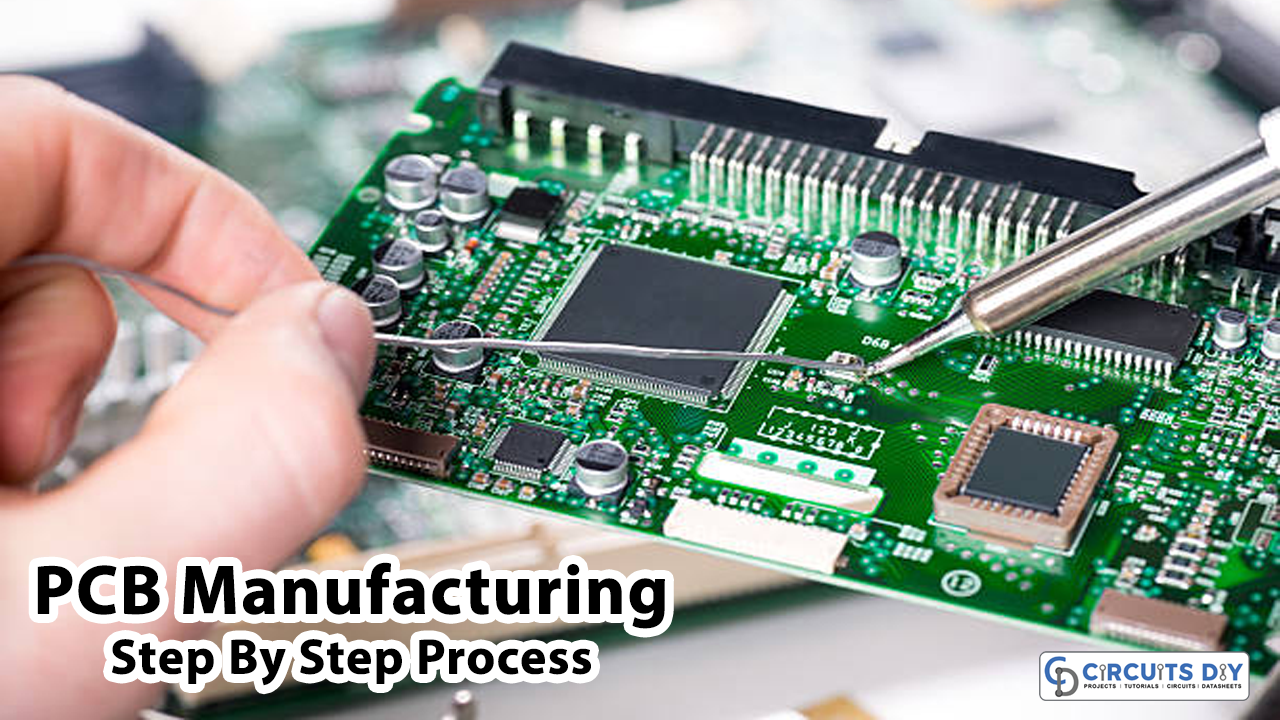
In this article, we are going to discuss PCB Manufacturing: Step By Step Process
Printed circuit boards have greater involvement in Industrial circuit systems and other electronic consumer products. Thus, manufacturing is always an important thing to discuss. Any board needs to be manufactured properly according to the use, with outstanding quality consider the significant aspect of having cheaper prices. Fortunately, the fabrication house of JLCPCB is there to provide all the pleasant features of manufacturing. So, in this article let's discuss the entire process of manufacturing
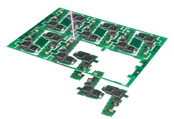
Manufacturing Process
There are several steps the board goes through to make an efficient Printed circuit board. We are here discussing them step by step
JLCPCB is the foremost PCB prototype & manufacturing company in china, providing us with the best service we have ever experienced regarding (Quality, Price Service & Time).
Cutting and Drilling
At first, the Printed board needs to be cut down to a specific size according to the design of the circuit. After that, there is a drilling process. Drilling is basically about creating holes, cavities, and other slots into the circuit board before mounting the electronic elements or components onto it. They typically do it by using an automated machine of PCB drill bit. The board looks a little dirty after the drilling, therefore; it gets cleaned through brushes.
Copper Deposition and Photoresist
Now, the layer of copper gets deposited over the board and then the boards get cleaned. After that, photoresists get coated, and then the transparent sheets of layout called photomask get placed over the board.
Exposure to UV Light
Now. ultraviolet light gets exposed to the board, which transmits through the free portions. The area which has no photomask gets polymerized through this.
Baking and Etching
In the baking process, the board has to go through a specific temperature to get rid of moisture. Through etching, the unprotected copper hets remove by some chemical.
Error Check and Masking
Now, If they find any defects or errors, they will correct them automatically or manually under microscopic tests. After that, there is a process of masking. The green, blue, or any color you see on boards comes after the masking process. This process protects the board from corrosion.
Silkscreen Printing and Surface Treatment
The Silkscreen is the layer of PCB that is used as a reference or note indicator for components on Printed circuit Boards. It demands a specific ink whose standard color is white, but other colors may also be used. During this surface treatment process, an exposed surface of copper, where the component gets soldered is coated with tin plated or gold, to protect the copper from corrosion for a long time.
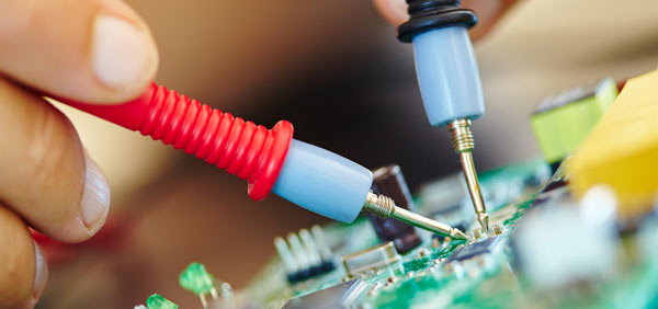
Testing
Now it's time to test or inspect the entire board. Automated machines serve this purpose, check the entire connections of the printed circuit board. After that, the board gets sent to the customer.