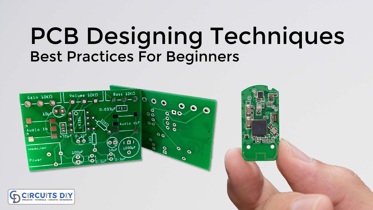
In this article, we are going to discuss PCB Designing Techniques Best Practices For Beginners
Proper PCB Designing techniques are an integral part of the production of every electronic gadget, which is used either for domestic use or for industrial purposes. Apart from electrically connecting, it also gives mechanical support to the installed electrical components.
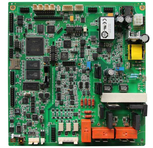
Usually, we Engineers, tend to pay most attention to circuit components, and code, but sometimes a critical component of electronics, the PCB layout, remains in neglect. Poor PCB design can cause function and reliability problems. If this is your first-time performing PCB designing, then seeing a chaotic-looking rats' nest might be a little intimidating. Below are the top 6 PCB Designing Tips that can help your PCB projects to run smoothly.
JLCPCB is the foremost PCB prototype & manufacturing company in china, providing us with the best service we have ever experienced regarding (Quality, Price Service & Time).
PCB Designing Techniques & Best Practices
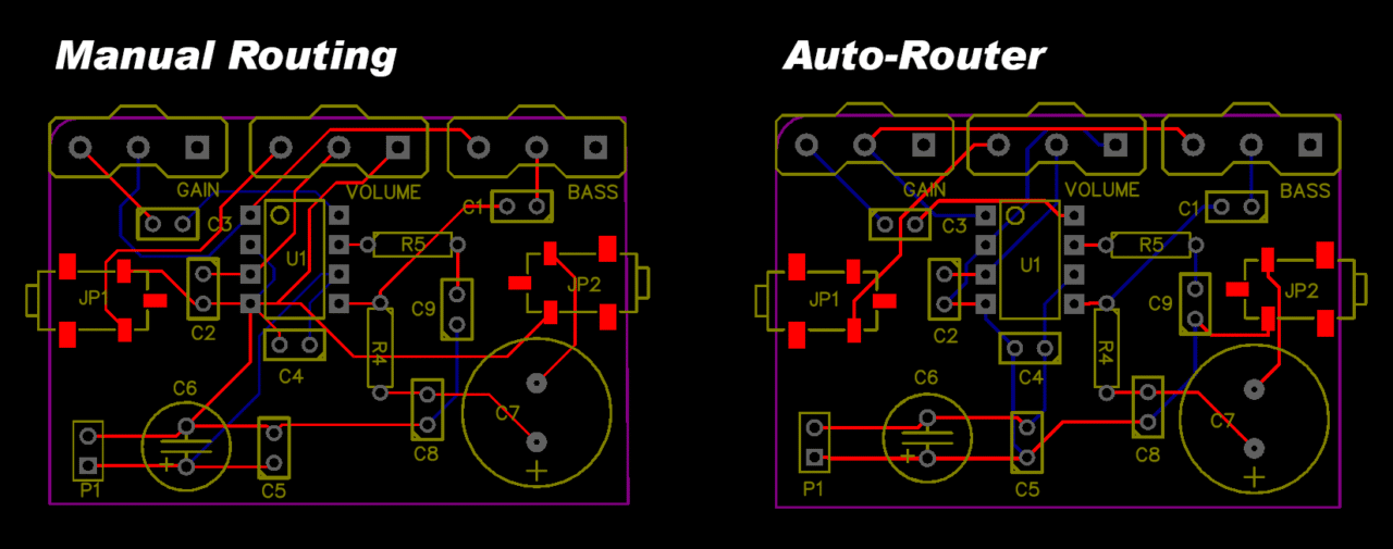
1) Manual Routing Over Auto-Routing
Use manual routing as much as possible. CADs are not more intelligent than the human mind. Unless it is very difficult, like multi-layer PCB with dozens of ICs, use hand-routing. It will be a much cleaner and neat design at the end.
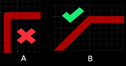
2) Use 45° Trace Angles
Designing with angles greater than 90 degrees can enable acid traps which can be harmful to the circuit board. Utilizing 45-degree angles are better practice as they have a smaller impact on the width of the trace. Narrow angles can cause electromagnetic radiation and copper migration over time and should be avoided.
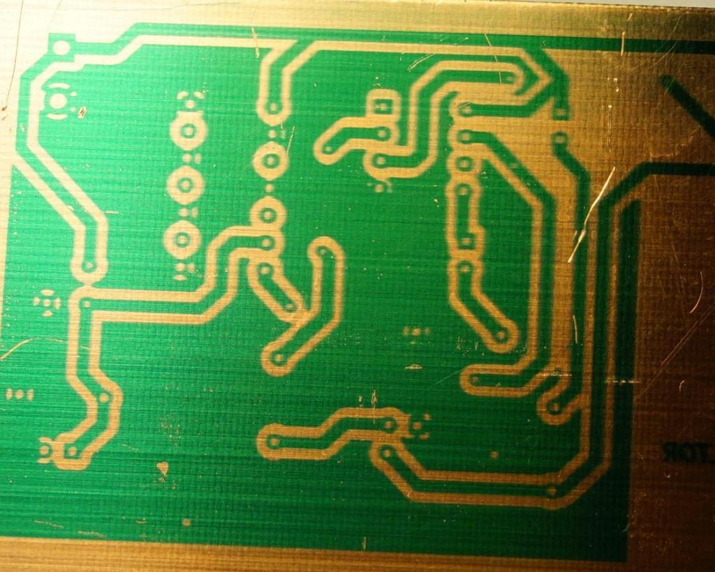
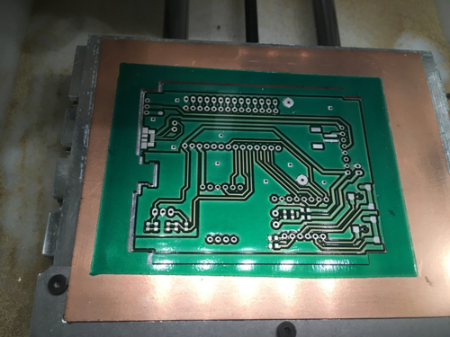
3) Make Clean & Smooth Copper Foil Traces
When drawing copper foil traces for printed boards, the shape of the copper foil of the printed board should be as compact as possible in order to avoid sharp corners & burrs. While the ends and corners of the copper foil should be as round, and chamfered as possible. It should be designed with neat and smooth trace lines. This is because sharp corners, burrs, and other dust, moisture, etc. often form sparks and discharges, causing faults such as leakage and short circuit.
4) Keep In Mind the Final Product Housing
Always keep the housing of the final product in mind when designing. Often, when we design PCBs we have no housing decided. But at the end of the day, the PCB needs to be in proper housing. So keep mounting holes there, choose some readily available and simple housing, and design the PCB around that. It is possible that later on the same housing gets approved and the re-designing is avoided.
5) Placement Of Heat Sensitive Components
Another important PCB design technique is to place components that are sensitive to heat away should be away from other components that generate heat. Examples of components that are sensitive to heat include thermocouples and electrolytic capacitors. Placing thermocouples close to heat sources may scramble temperature measurements. Placing electrolytic capacitors close to heat-generating components will reduce their operating life. Components that generate heat may include bridge rectifiers, MOSFETs, inductors, and resistors.
6) Use Solder Mask
Use solder masks in all of your PCB designs. The savings from omitting the solder mask are slight but the risk of short circuits in the soldering process is much greater.