Part one of a series on how to build your own computer from scratch, based around the Z80 CPU.
In this series, Robin builds a Z80 computer from scratch. Catch up in the table of contents below:
Introduction
When people say that they've built their own computer, what they really mean is that they've taken an off-the-shelf CPU, plugged it into a motherboard, added the extra peripherals, and then hit the "on" button. This isn't really building a computer so much as it is assembling a computer.
In this DIY Hacking series, we will actually build a computer based around the Z80 CPU. In the process, we'll learn how it works and how to program it!
The Z80 processor was designed by Zilog (led by Federico Faggin) and first hit the shelves in 1976. It was a direct competitor against the popular Intel processors, offering both compatibility with Intel systems and also more functionality.
Just some of the features that made the Z80 vastly superior to other CPUs on the market at the time included extra registers, more instructions, a less complicated IO (i.e., single clock input and single rail supply), and a better interrupt system.
Before we can go further into detail, it is imperative that the following topics are well understood as this project will require some knowledge on computers, microcontrollers, and circuitry.
Understanding the Physical Processor
Assuming that you understand the topic list above, let’s get started with the Z80 IC, itself.
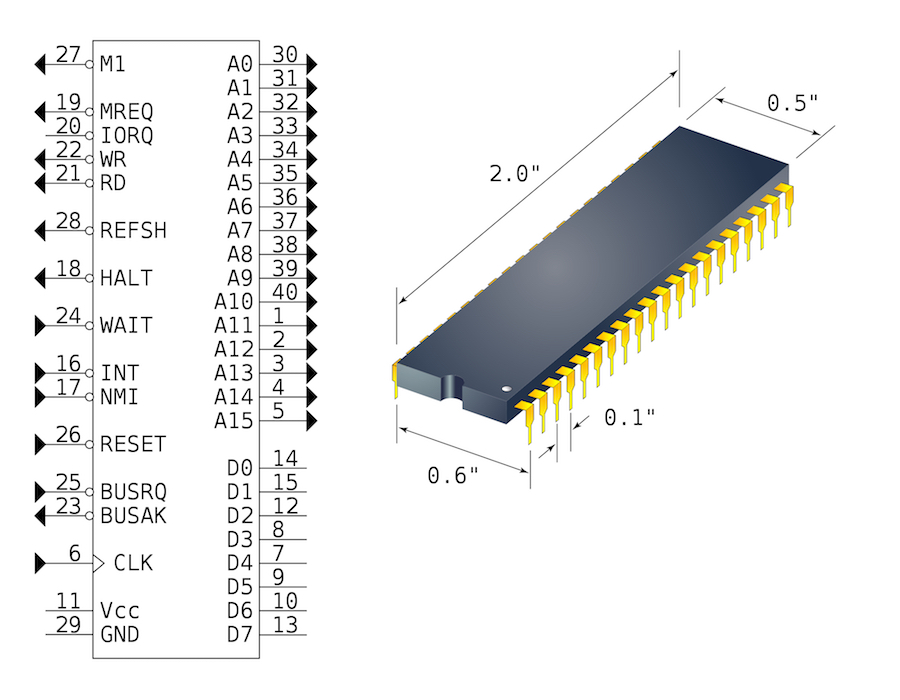
The Z80 processor is an 8-bit CPU with an 8-bit data bus and a 16-bit address bus. This means that the Z80 can read or write up to 8 bits at a time while being able to access up to 65536 individual locations by using the address bus.
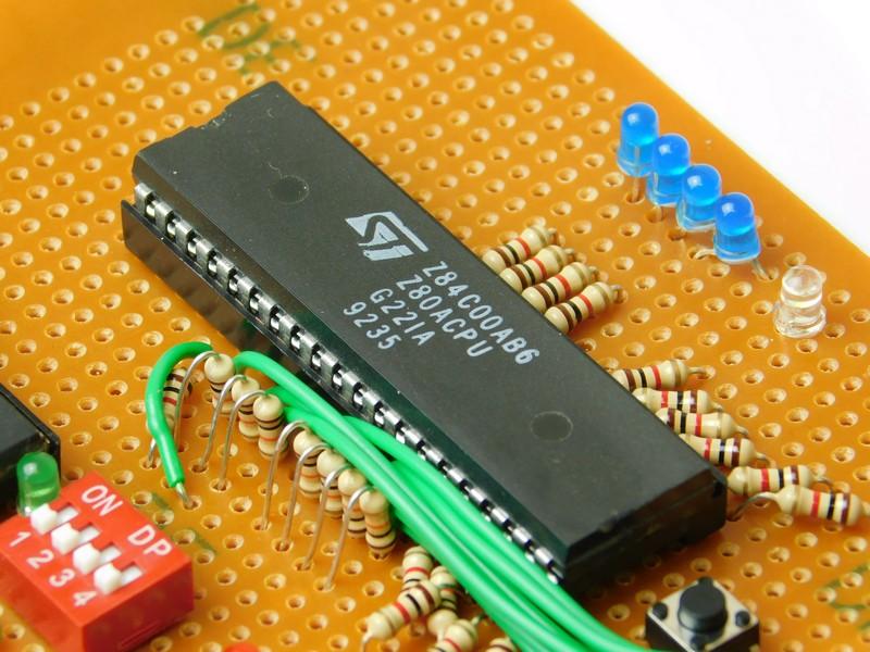
The processor is commonly found in a 40-pin DIL package, which makes it very hobby friendly for those who want to use strip boards, breadboards, and matrix board.
Considering that this is the first time you will be using the Z80, it is advised that you use a breadboard for this project as it will allow you to make changes with ease.
The address pins on the CPU are labeled as A with the range of addresses including A0 to A15 (A0 is the lowest significant bit with A15 being the largest significant bit). The data bus pins on the CPU are labeled D with the range of data bits including D0 to D7. However, connecting these pins up to external devices will prove pointless if the other pins on the processor are not dealt with.
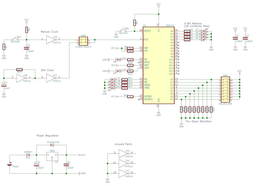
The first pin we will look at is probably the most important, the clock line. This pin takes in a single phase clock signal whose frequency can range from 0Hz up to 4MHz (the upper limit depends on your specific processor). Typically, this pin will connect to a clock source but in this project we will connect it to a debounced switch circuit so we can step through programs to see how the processor operates.
The next few pins to look at are the memory and IO control lines which enable us to select what kind of device we want to connect to. These pins are RD, WR, MREQ, and IORQ with all of these pins being outputs. The Z80 can access either RAM (memory) or IO devices (e.g. keyboard), and this selection is made by driving MREQ or IORQ low (0V). If MREQ is low then the Z80 is trying to access RAM and if IORQ is low then the Z80 is trying to access an IO device. If RD is low then the Z80 is trying to read from that selected device and if WR is low then the Z80 is trying to write to that device. Currently, we do not have any devices so we will just connect these to some LEDS to see how they behave during instruction cycles.
One pin that will be very helpful in particular is RESET which is an input pin that must be tied to 5V using a 1K resistor. If we connect the RESET pin to 0V and send a minimum of 4 clock pulses the processor resets itself which resets the registers, program counter, and other internal states.
Two output pins that will be helpful in our test circuit are HALT and M1 which will both be connected to LEDs for indication. If the Z80 is about to start a new instruction then M1 will go low (0V) and if the HALT instruction (0x76) is executed by the processor, the HALT pin goes low.
Some of the input pins will not be considered in this tutorial as they are only important in high end Z80 computers and these pins are WAIT, INT, NMI, and BUSRQ. For now, connect all these pins to 5V using a 1K resistor. There are also output pins that will not be used as they are either advanced (BUSAK) or now redundant (REFSH). These can be ignored for the time being!
Z80 Computer Schematic
Understanding the Machine Cycles
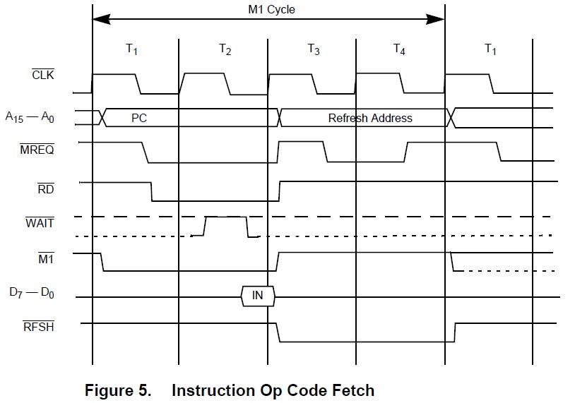
If you have built the circuit correctly and have applied power (with the clock selector selecting the manual clock circuit), you should see all of the control LEDs on (WR, IORQ, HALT, MREQ, M1, and RD). Assuming that the Z80 is in its correct RESET state, the first push of the clock switch should result in M1 going low. M1 indicates that the Z80 is going to perform an instruction that it will try and read from RAM but since we don't have any, we will just instead feed the NOP instruction to the Z80 by setting all the switches on the data bus off so that the data value on the Z80 bus should read 0x00. Since the processor is trying to read from RAM, MREQ and RD also go low. Despite that the RD and MREQ lines are low, the data on the bus can still change at this point. When we push the clock switch again, the data that is present on the databus is latched into the Z80s internal instruction register. Pressing the clock switch twice at this point will get the Z80 to both process the instruction and go through its refresh cycle (this was needed for DRAM in the past where data had to be refreshed frequently). As we set the databus to the NOP (No Operation) instruction the Z80 will simply move on and start the cycle all over again. This cycle is called the Instruction Fetch as the processor is “fetching” an instruction from memory to perform!
Image courtesy of Zilog (link downloads PDF)
Because our basic computer lacks IO or memory, sending instructions to the Z80 is rather difficult. However, there is one other instruction that we will send to the CPU which will produce an interesting response: HALT.
When this instruction (0x76) is executed, the Z80 processor halts and performs internal NOPs until an external interrupt is detected (a low signal on either INT or NMI, however, we will not cover this further). Since we have the HALT pin connected to an LED, the execution of the HALT instruction show turns this LED off.
Construction
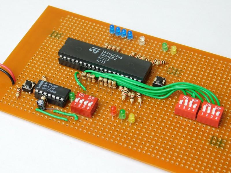
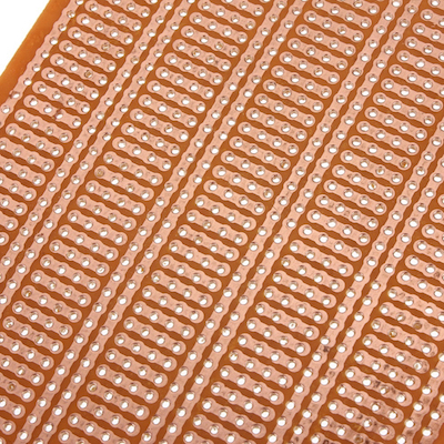
Z80 projects are usually very difficult and prone to error which is why it is advised that a prototyping construction method is used. For example, stripboard and breadboard are ideal construction methods whereas matrix board and PCBs are not. The best stripboard for such projects are those that contains separated pads with common power lines (as shown below).
Check out the video below to see the project in action:

