Introduction
[Update 08/23/2021: The PCB layout has been improved and made much more compact. Also, the number of analog inputs has been decreased from 32 to 16.]
There's often the need to measure a bunch of analog signals, and in order to make accurate measurements, we may resort to adding an external ADC to our existing microcontroller system to provide more resolution.
This project features the PIC18F4550 and the ADS8326.
Getting Started
The first step is to come up with a suitable architecture that's going to meet our needs. For this design, it is desired to have access to 16 analog channels and "really good" resolution. I felt that, an ADC with a 16-bit resolution met the threshold of being good enough.
For the main controller, I wanted to go with one that had enough community support and was relatively easy to use. Obviously, there are many options out there that could have been chosen, ultimately, I went with the PIC18F4550 because it seemed like a good fit. Also, I have never used PIC microcontrollers for any of my designs—so why not try something new?
Notice that I have not mentioned an specific application for this data acquisition system. The reason being that it could be used to measure any analog signal (within our specs) coming from devices such as thermistors, pressure sensors, and actually, any analog input we'd like to process in the microcontroller. You will notice, though, that the design focuses on measuring temperature through thermistors since that was the original intended application.
System Architecture
Here is a high level view of the data acquisition system:

The ADC is the ADS8326. This is a 16-bit, single channel SAR ADC, with an SPI bus to stream its output data. It offers high throughput (spec'd at 250,000 samples/sec max) and comes in a small package size.
You will also notice the use of a 16x1 mux. Given the fact that the ADS only has one channel, we need a way to connect all the 16 analog inputs to the ADC's single input—so the 16-channel mux allow for that at the expense of requiring extra pins for the select lines S0 through S3, and the enable pin. Keep in mind, that this is an analog mux that ideally propagates the analog signals exactly as they appear at its inputs. Of course, there are side effects such a noise that we need to deal with and hopefully calibrate them out of the system.
Schematic Part

This is a complete schematic of the system. I have added other components such as LEDs and headers, to allow for debugging. I've brought out some of the unused pins of the PIC18F4550, so that they can be tapped into if needed.
To add more options and/or debug capabilities, I've also exposed the PIC18F4550 on-chip USB interface; this provides with more ways to output relevant data through a serial terminal program, for example.
There is a 32-position header intended for connecting the external analog inputs. You will notice a bunch of 10k resistors, pulling one side of the headers up to 5V. Initially, the circuit was designed to measure temperature values, by using thermistors. These thermistors have a nominal resistance of 30k at 25°C. When connected appropriately to the header, the thermistors will form a voltage divider with the fixed 10k ohm resistor and at 25°C, the voltage drop across the thermistors will be 3.75V.
PCB Layout
There are different ways to lay out the PCB. One thing to always keep in mind: Whenever there are analog signals to be measured, they need to be kept away from the digital signals. Digital signals are inherently noisy, and can have an adverse effect on the analog measurements.
There's a wealth of online resources on mixed signal PCB techniques. Feel free to look into some of them as necessary.
Here is a picture of an actual board:

Some Coding
Now that we have some hardware, it is a good idea to test the basic functionality of the board. At the heart of the source code, we have the SPI engine, which allows to read the data from the ADS8326.
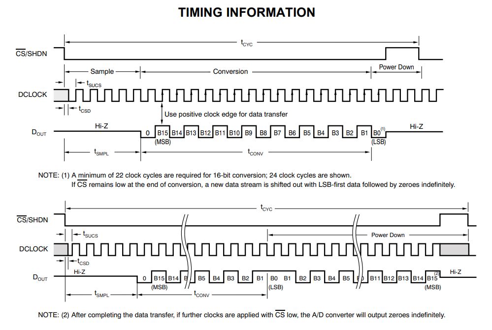
The PIC18F4550 has an on-chip SPI interface that we need to properly set up. Looking at the ADS8326 timing diagram, there are a couple of things to pay attention:
- After asserting the CS line (active low), it takes about 4 to 5 clock cycles (line is held in Hi-Z) before meaningful data is shifted out of the slave (ADS8326) into the master (PIC18F4550)
- The data always starts with a '0' (or 0V)
- The data needs to be sampled at the rising edge of the clock
Item (1) makes it necessary to hold the data line in some known state. That way, we could distinguish when actual data is being streamed into the microcontroller (if it is Hi-Z, we don't know what the state could be). It makes sense to pull the data line up to 5V (e.g. use a pull-up resistor! I missed that in the design and struggled to detect the start '0' bit consistently) so that when we see the first '0' on this line (2), it indicates to us that the next 16 bits are the ones to be recorded.
There are many tutorials online on how to set up the PIC18F4550 in SPI mode, so I am just going to drop here an actual implementation. In this case, I have the SPI set to clock the data out (bit by bit) from the ADC at 1.25MHz:
byte SPI_Read(byte *arr, unsigned int length){
    PIR1bits.SSPIF = 0;
    SS = 0;
    byte tempvar;
    tempvar = SSPBUF;

    for (unsigned int i=0; i<length; i++){
        SSPBUF=0xff;               /* Copy flush byte in SSBUF */
        while(!PIR1bits.SSPIF);	  // Wait until the receive flag is 1
        arr[i] = SSPBUF;          // Read the buffer
        PIR1bits.SSPIF = 0;       // clear the receive flag
    }

    SS=1;
    __delay_us(100);
}
I also wrote a function to read specific analog inputs. For that, we need to enable the corresponding mux and select the desired input by driving S0, S1, S2, and S3 to the right levels.
unsigned int readExtADC(unsigned int channel){
    byte arr[6] = {0};
    byte tempvar = 0;
    byte check = 0xff;
    byte s = 0;

    unsigned int adc_value = 0;
    if (channel<=0 || channel>16){
        channel = 1;
    }
    EN = 0;
    switch (channel){
       case 1: S3=0; S2=0; S1=0; S0=0; break;
       case 2: S3=0; S2=0; S1=0; S0=1; break;
       case 3: S3=0; S2=0; S1=1; S0=0; break;
       case 4: S3=0; S2=0; S1=1; S0=1; break;
       case 5: S3=0; S2=1; S1=0; S0=0; break;
       case 6: S3=0; S2=1; S1=0; S0=1; break;
       case 7: S3=0; S2=1; S1=1; S0=0; break;
       case 8: S3=0; S2=1; S1=1; S0=1; break;
       case 9: S3=1; S2=0; S1=0; S0=0; break;
       case 10: S3=1; S2=0; S1=0; S0=1; break;
       case 11: S3=1; S2=0; S1=1; S0=0; break;
       case 12: S3=1; S2=0; S1=1; S0=1; break;
       case 13: S3=1; S2=1; S1=0; S0=0; break;
       case 14: S3=1; S2=1; S1=0; S0=1; break;
       case 15: S3=1; S2=1; S1=1; S0=0; break;
       case 16: S3=1; S2=1; S1=1; S0=1; break;
      }

    SPI_Read(arr,6);
    tempvar = arr[0];
    while(tempvar!=check){
        tempvar = (tempvar>>1);
        check = (check>>1);
        s = s + 1;
    }

    check = 0xff;
    check = (check>>(8-s));
    arr[0] &= check;

    arr[2] = (arr[2]>>(s-1));
    adc_value = (arr[0]<<(16-s+1)) + (arr[1]<<(8-s+1)) + arr[2];

    return adc_value;
}
You notice that at the end of the readExtADC() function, we do some bitwise and shifting operations. Those are required in order to extract the actual data from the ADC. Recall, that the ADC needs some time (sampling time) to read the analog input—about 5 SPI clock cycles. During that time, the ADC's SDO line is in Hi-Z but since we have a pull-up resistor, we'd read 1's until, the first '0'—which signals, that the next 16 bits are meaningful. So we need a way to discard the first 1's that don't mean anything to us and that's what is accomplished by the bitwise and the shifting operations.
Some Results
After running some tests and adjusting a few things in the code, I could get a basic program to exercise ADC operation.
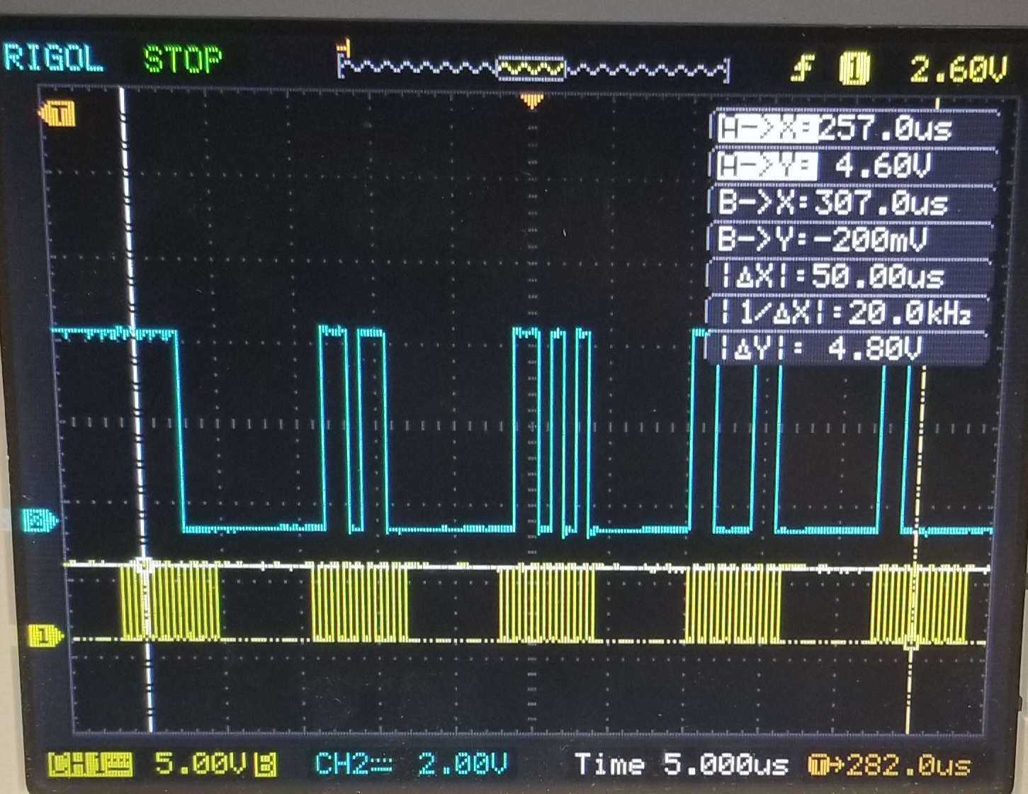
Here is a picture of what the signals look like in the oscilloscope:
SPI Signals. Yellow is clock @1.25MHz and blue is the actual data being transmitted from the ADC
The SPI clock is in yellow and the actual data signal is in blue. As shown, there are 6 intervals where the clock is active (oscillating). These are the intervals where we are reading the data (in blue) into the PIC18F4550 and each interval corresponds to reading 8 bits (1 byte).
We don't actually need to read 6 bytes, but we know that for sure we need to read at least 3 bytes—recall that after the first '0', the next 16 bits are the ones we're after. Now, the first '0' could happen after we receive five or six successive 1's in the first byte. This means that the third byte will contain some of the bits (LSBs) that are still part of the 16-bit stream. For example, if 11110101 is received in the first byte, we know that the first four 1's need to be thrown away, and the actual data, we can get out of the first byte, is just 3 bits (101). The second byte will provide 8 more bits, and the third byte is necessary since it contains the remaining 5 bits that complete the 16-bit transmission.
Improving the Measurements
Depending on the application, we may want to calibrate our system in order to mitigate the effect of noise. Before the signal gets to the ADC's input, it has to pass through the mux and the buffer OPAMP. Those add noise and uncertainty to the measurements, and in some cases, it may be necessary to counteract those.
One way, and probably the simplest approach, is to take a bunch of samples and take the average of those. That should filter out most of the high frequency noise. It makes sense to do this, when the dynamics of whatever is being measured should not be changing quickly—that is the case for temperature measurement, temperature should not change drastically over short periods of time. In code, this could be achieved by doing something like this:
#define NUMBER_OF_SAMPLES_AVG 100
unsigned long int sum = 0;
for (byte n=0; n<NUMBER_OF_SAMPLES_AVG; n++){
	sum = sum + readExtADC(1);  // Read channel 1, and add to previous reads
}
adc_values[i] = sum/NUMBER_OF_SAMPLES_AVG;
sum = 0;
That piece of code will take 100 samples and average them out. The downside of the average approach is that it takes more time but it may acceptable depending on how fast the measurements are needed. We can always increase the SPI clock (up to 6MHz for the ADS8326) to help with that.
Another approach but more complex, is to characterize the noise. This could be done by applying a precise variable voltage source the at one of the channels and sweep voltage values, say, from 1V up to 5V. For each input voltage, we know ideally what the ADC should read. As the input voltage source is swept across the operating range of the ADC, subtract the actual ADC code (read by the microcontroller) from the ideal code, and record all of those errors.
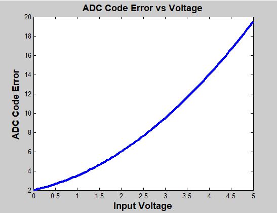
Once the error is quantified, it is a good idea to plot it and see what it looks like. Does it look linear? Non-linear? Constant offset? This will provide us with some intuition of how to characterize it. The next step involves a finding a linear regression fit, to describe the noise function. For example, say that as the variable voltage source is swept, the error looks like this:
It shows that the error has an offset of 2 codes. That means that if 0V is present at the analog input, instead of getting the 0x0000 code from the ADC, it will actually send the 0x0002 code. If the voltage source is swept all the way up to 5V, the error grows with what appears to be a combination of linear and non-linear terms. The error could then be modeled as:
e = a + b*ADC_CODE + c*ADC_CODE^2
The coefficients a, b, and c need to be found. We know a=2 in this example, but in general, all three constants could be found using linear regression techniques. That is, however, beyond the scope of this article but at least provides a place to start.
Once an appropriate model for the error has been found, then the actual code can be corrected, by subtracting the error function:
ADC_CODE_CORRECTED = ADC_CODE_READ - e
There are more involved ways to improve the measurements but I feel most of the times, it suffices to use the two methods explained in this section, or a combination of both.
Conclusion
Data acquisition systems need to offer quick and accurate measurements in so many applications. Their design is nontrivial and requires knowledge of many aspects of electronics.
I sure hope that this was an interesting reading and don't hesitate to make suggestions, comments, and/or ask questions.