Now that we've learned all about Panelizing, dive deeper and get to know the different types of how to Panelize PBCs!
If you are developing a product that contains electronics on a PCB, a manufacturing technique called panelization will likely be important to learn as your product moves towards production at scale.
Panelizing PCBs involves connecting multiple boards together so that they can be manufactured all at once. The boards are connected in ways that allow the individual PCBs to be easily separated after they are manufactured and assembled.
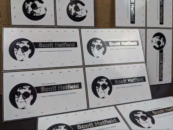
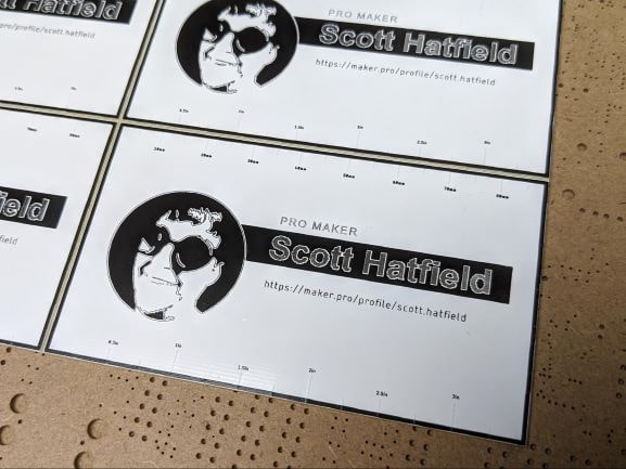
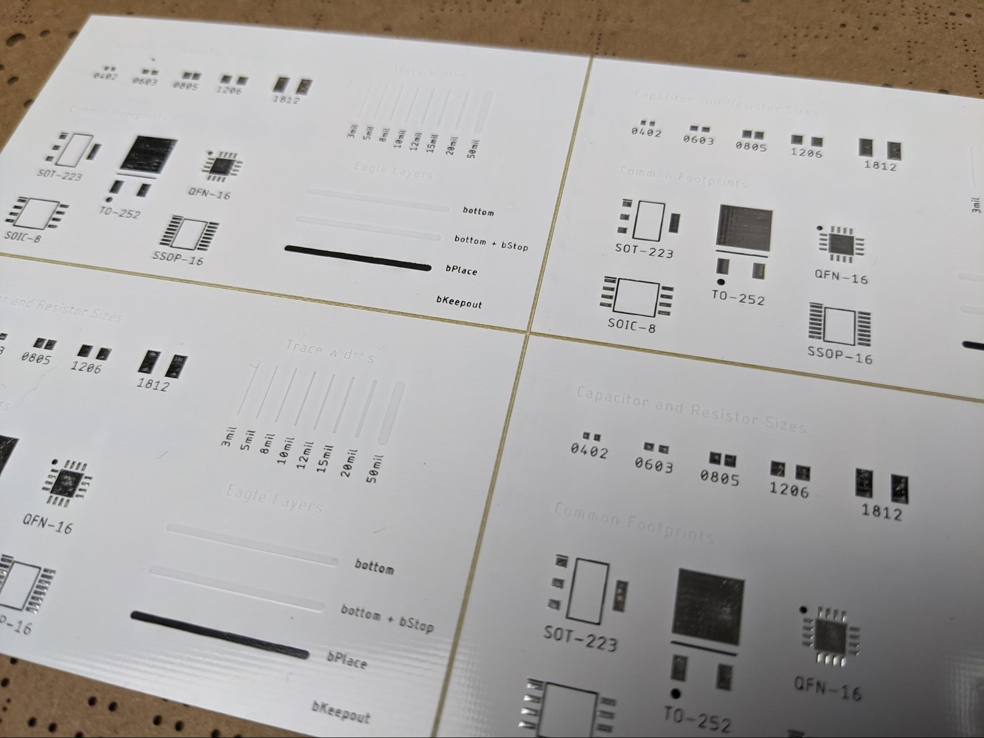
These are PCB business cards that were manufactured in a 2x2 panel
Panelizing PCBs is advantageous because it allows multiple PCBs to be assembled at once, which reduces the per-part cost of assembly. Plus, in some cases, for example, if your board is small, panelization may be required in order to end up with a board size that is supported by your PCB manufacturer.
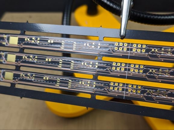
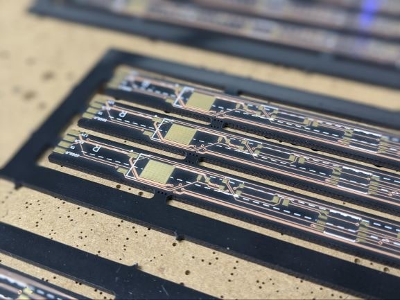
These thin PCBs were placed into a panel in order to make the entire panel large enough to manufacture
In this article, the second in the series, we’ll look at the two main types of PCB panelization, exploring how they work, and when each type would work best.
Types of Panelization
There are two main types of PCB panelization: V-groove panelization and tab-route panelization. These two methods join PCBs together in different ways and you might choose one over the other based on the design of your PCB.
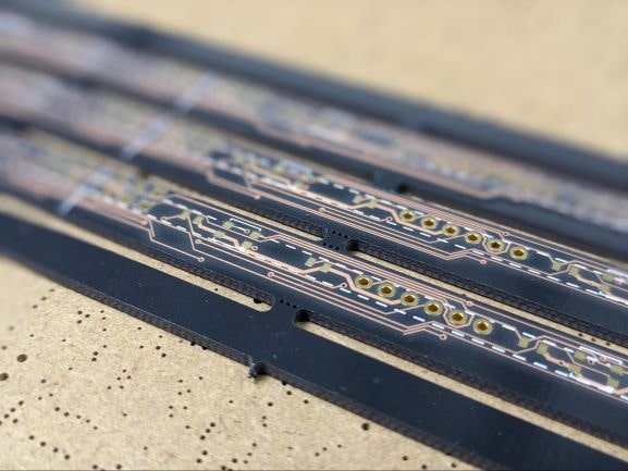
This is a tab-route panel
V-groove Panelization
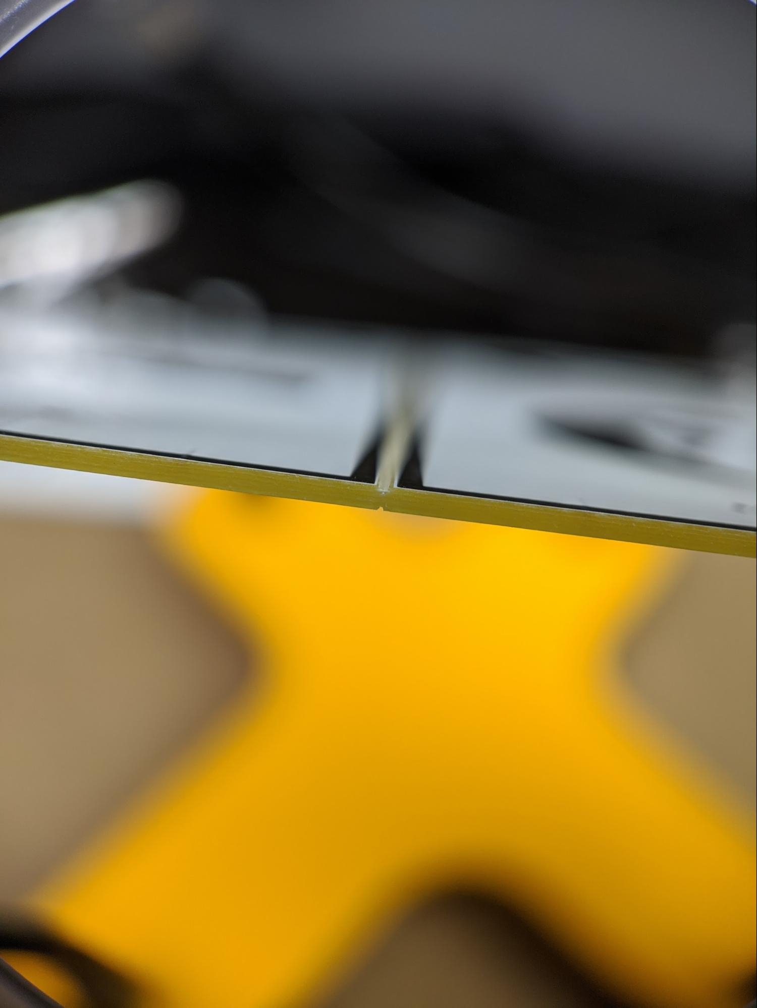
In V-groove panelization, a triangular saw is used to cut about one-third of the way through both sides of the panel. This leaves a thin section of FR4 holding the individual PCBs together so they can be separated with simple tools.
Viewed very closely from the end of the board, you can see where a V-groove saw has cut partially through the PCB from each side
Because a saw is used, V-groove panelization can only be used in designs with straight lines separating the PCBs. The V-groove cuts must also extend from one edge of the board to the other.
V-groove panelization cannot be used if there are parts overhanging the edge of the board, because the saw could hit these overhanging parts which would obviously be a bad thing.
The yellow color of the FR-4 is visible in the lines cut by the V-groove saw
V-groove panelization has the advantage of being much faster than tab-route panelization. It takes a fraction of a second for each board to pass under the V-groove saw. Another benefit is that the V-grooves add negligible additional space to the overall size of the panel, which reduces costs.
Tab-Route Panelization
For PCBs that cannot be separated by simple, straight lines or for designs involving multiple different PCB designs, tab-route panelization offers a more flexible panelization strategy.
In tab-route panelization, a router is used to cut through the FR4 between boards. Small tabs are left to hold the boards together during assembly. These tabs can then be broken apart using depanelization tools, or carefully by hand.
This is a tab-route panel in which the individual PCBs are connected by perforated tabs
Tab-route panelization also allows for boards that have parts overhanging the periphery of the board. For example, many designs with USB ports are designed such that the port sticks out from the side of the board. This is necessary to plug in the USB cord. Designs like this cannot be panelized with V-groove panels because the saw blade will hit the USB connector.
Most of the time, the tabs on tab-routed panels are perforated with a series of holes to make it easier to separate the boards.
Depanelization
Of course, after your PCBs are manufactured in a panel and assembled with all your electrical components, they need to be broken apart into individual PCBs. This is not as simple as it might at first seem. Bending the boards and breaking them apart by hand places stress on the PCB and the components attached to it, especially components placed close to the edge of the board. This stress could potentially break solder joints and cause malfunctions in the circuit.
To avoid this issue, there are several tools commonly used to depanelize PCBs without putting too much stress on the board: guillotine cutters, wheel cutters, punches, and laser cutters.
For prototype boards in a panel, depanelization can be done by hand, as long as care is taken not to put too much stress on the PCB.
Fortunately, most PCB manufacturers will depanel your boards as part of their cost structure. However, it is still important to understand which depaneling method your fab is using so that you can make good design decisions when it comes to part placement and overall PCB design.