Learn all about DNPs or do not populate components, keeping designs modular and reducing the risk of permanent mistakes!
Circuit board design can be a daunting process. Unlike breadboarded circuits or circuits made on perfboard, a custom printed circuit board is much less modular.
Mistakes on a PCB may be more difficult to fix. Certain circuits that use devices in unfriendly, small packages or devices sensitive to their circuit board layout may not even be possible to prototype without a custom printed circuit board. However, steps can be taken to make this process less daunting and risky.
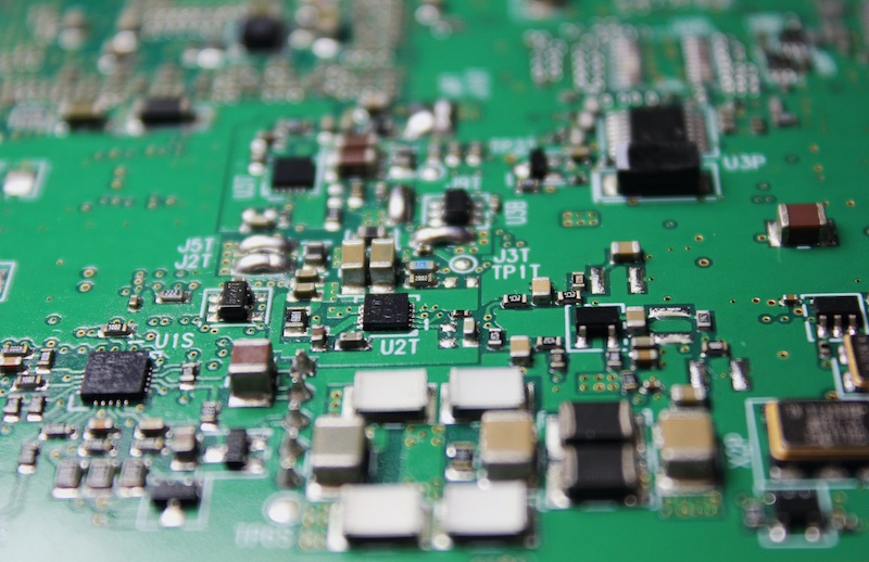
DNP components (which stands for do not populate or do not place) refers to the components designed into a circuit that aren’t placed right away — if at all — on the actual board. Incorporating these components into a design allows for a modular PCB design with easier rework.
Using the Same PCB for Many Applications
PCB layout isn’t everyone’s favorite hobby. Designing a board to work for multiple applications can limit the amount of time spent in front of the computer, saving more time for the bench!
Several projects might use the same microcontroller, or WiFi/Bluetooth transceiver, but require different sensors or actuators. One board can be designed that includes circuit pads and connections for all of these devices, but only certain ones will actually be soldered to the board for different applications. One microcontroller peripheral — such as a certain GPIO pin, analog input, etc. — can even be hooked up to multiple devices as long as only one is populated at a time.
However, when designing one board for multiple applications, extra care should be taken to ensure leftover circuit “stubs” won’t cause any issues. Stubs are circuit traces that are only connected at one end. An unpopulated circuit amounts to just that: circuit traces that lead to nowhere. These traces could be a potential point of failure in high-speed digital applications, such as USB. Stubs present on these signal lines can cause signals to be reflected back through the line, corrupting the information embedded in them.
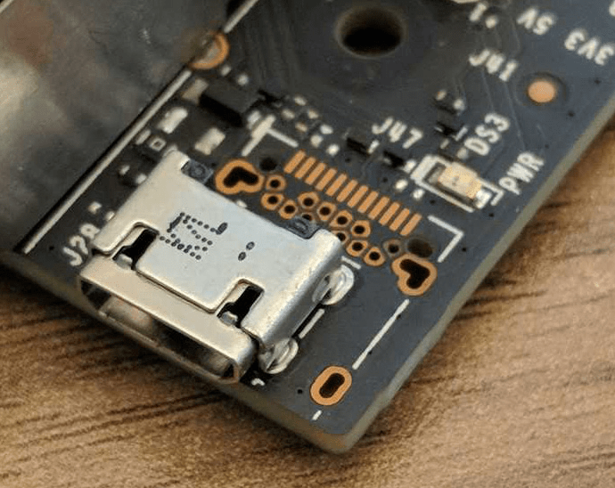
The NVIDIA Jetson Nano board ships with a micro USB connector, but it also has the footprint for a USB-C connector, which can deliver more power than micro USB.
Testing Other Configurations
Choosing whether or not to populate certain components allows the circuit designer to change the functionality of their circuit without designing a brand new board. For a board with one application or multiple, leaving DNP component pads can make the design process faster and easier, and at a reduced cost, by enabling prototyping on a custom PCB. It also enables the designer to simplify their circuit debugging process and limit the amount of complicated rework they have to do.
DNP Components in Power Supply Design
DNP components can be helpful when designing a power supply. Circuits that are prone to experiencing transients, where the current demanded by the circuit abruptly spikes very high, may require extra capacitance to operate properly.
Even if a power supply is rated to handle a certain peak current, its output voltage may not remain stable during a very fast, high transient. This can be compensated for by adding extra output capacitance. Instead of testing many different capacitors, the PCB designer can leave pads for several capacitors in parallel.
The engineer also won’t need to risk damaging the board by constantly soldering and desoldering one capacitor. For anyone who has ever accidentally ripped a surface mount pad off of a board while reworking, this can save a lot of frustration. As an added bonus, several capacitors in parallel will have a lower ESR (equivalent series resistance) than a bulk capacitor.
DNP Components in Matching Network Design
Another use case for DNP components is in matching network design. Without diving too deep into the details of radio frequency (RF) design, many antennas — such as PCB trace antennas used with Wi-Fi devices like the ESP8266, or Bluetooth devices like the nRF52 family — require an impedance matching circuit, consisting of capacitors and inductors, between the antenna and the device using it.
A product’s enclosure and the environment it is used in will affect its wireless performance, so simply calculating the best component values using the datasheet may not be adequate for optimal performance. Designating some of these components as DNP enables a more complete antenna matching/tuning process, allowing for different component values and configurations to be tested.
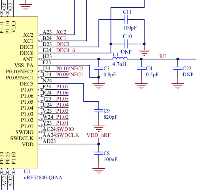
The nRF52840 reference schematic. C22 is DNP for antenna tuning, and C10 is DNP for optional power supply decoupling. Detail of schematic from Nordic Semiconductor.
Separating a Load
When designing a power supply, it can be helpful to have the ability to separate the supply from its load (the devices that it will be supplying current to). A common way to do this is to place pads for a 0-ohm resistor (sometimes called a jumper), between the source and load.
Circuits like buck and boost converters aren’t simple to prototype on a breadboard. One reason for this complication is that the ICs are typically small and surface mounted. Even if an adapter board is used, these circuits need to be laid out with precision for the best performance, requiring a PCB.
When using an unfamiliar device or testing a new power architecture, an unpopulated jumper allows the designer to test and debug the supply’s output before exposing it to potentially sensitive devices, which could be damaged in the event of a design flaw.
After applying power to the board, the power supply circuit’s output can be checked with a multimeter. The designer could also consider adding in a “dummy load” resistor (another DNP component!) intended to ensure that the circuit can maintain a steady output voltage while supplying current. After verification, the optional load resistor can be removed and a 0-ohm jumper (or simply a solder bridge) can connect the power supply to the rest of the circuit.
DNP Components Offer a Useful Tool
DNP components can be a useful way to make sure that your board works the first time, or to prototype designs with difficult-to-use components. It can save time and money by limiting design iterations and allowing one board to serve multiple applications. While it may seem obvious to a veteran designer, those new to PCB design may not have considered unpopulated components to be an acceptable option in design, but they are truly a valuable tool.