Make your own printed circuit board at home to reduce problems that arise from loose connections on a breadboard.
If you are into electronics, PCBs are some of the most common things you will see. These boards make our lives easier by eliminating all those connecting wires and breadboards. If properly designed, it will reduce the size of your device and can look very sexy.
What is a circuit board?
A printed circuit board (PCB) mechanically supports and electrically connects electronic components using conductive tracks, pads, and other features etched from copper sheets laminated onto a non-conductive substrate. A printed circuit board has pre-designed copper tracks on a conducting sheet. The pre-defined tracks reduce the wiring, thereby reducing the faults arising due to loose connections. One simply needs to place the components on the PCB and solder them.
In this tutorial, I will show you how you can make circuit boards at home easily. Doing so will save you a lot of time from debugging and double checking the connections on a breadboard. You can even make your own Arduino after going through this DIY Arduino tutorial after this one. So, sit back and see how it’s done!
What are the different ways to make a Circuit Board?
There are in all three basic methods to make a PCB:
- Iron on Glossy paper method.
- Circuit by hand on PCB.
- Laser cutting edge etching.
Since laser method is the industrial method to make PCBs, we will go into detail for the first two methods.
PCB Design:
PCB design is usually done by converting your circuit’s schematic diagram into a PCB layout using PCB layout software. There are many cool open source software packages for PCB layout creation and design.
Some are listed here to give you a head-start:
- Autodesk Eagle
- PCBWizard
Designing a Circuit Schematic in Autodesk Eagle:
In Eagle: File> Export>ImageBe sure to set DPIG to 1200 for better quality
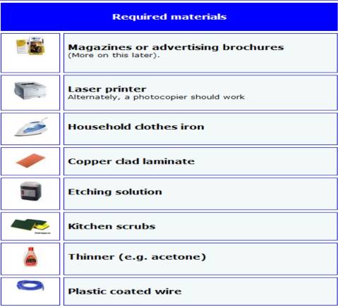
What Materials are Required to Make a Circuit Board?
You also need: FeCl3 powder/solution (same as etching solution), photo/glossy paper, a permanent black marker, a blade cutter, sandpaper, kitchen paper, and cotton wool.
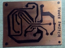
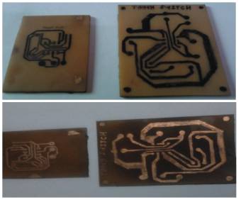
For this tutorial, let’s consider making a PCB for a simple project- a Touch Switch using IC555.
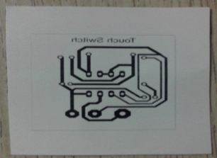
STEP 1: Take a printout of circuit board layout
Take a print out of your PCB layout using a laser printer and the A4 photo paper/glossy paper. Keep in mind the following points:
- You should take the mirror print out.
- Select the output in black both from the PCB design software and the printer driver settings.
- Make sure that the printout is made on the glossy side of the paper.
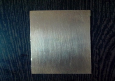
STEP 2: Cut the Copper Plate for the Circuit Board
Cut the copper board according to the size of the layout using a hacksaw or a cutter.
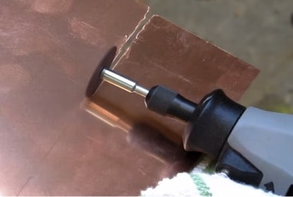
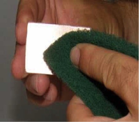
Next, rub the copper side of the PCB using steel wool or abrasive sponge scrubs. This removes the top oxide layer of copper as well as the photoresist layer. Sanded surfaces also allow the image from the paper to stick better.
Rubbing away the top oxide layer
STEP 3: Transfer the PCB Print onto the Copper Plate
Method 1: Iron on Glossy Paper Method (For Complex Circuits)
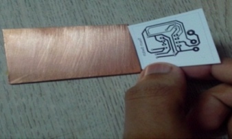
Transfer the printed image (taken from a laser printer) from the photo paper to the board. Make sure to flip top layer horizontally. Put the copper surface of the board on the printed layout. Ensure that the board is aligned correctly along the borders of the printed layout and use tape to hold the board and the printed paper in the correct position.
Place the printed side of the paper on the plate
Method 2: Circuit by Hand on PCB (For Simple and Small Circuits)
Using the circuit as a reference, draw a basic sketch on the copper plate with a pencil. Once your sketch looks good, trace over it with a permanent black marker.
Using the permanent marker to sketch the PCB
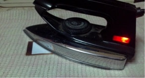
STEP 4: Iron the Circuit from the Paper onto the PCB Plate
- After printing on glossy paper, we iron it image side down to the copper side, then heat up the electric iron to the maximum temperature.
- Put the board and photo paper arrangement on a clean wooden table (covered with a table cloth) with the back of the photo paper facing you.
- Using pliers or a spatula, hold one end and keep it steady. Then put the hot iron on the other end for about 10 seconds. Now, iron the photo paper all along using the tip while applying a little pressure for about 5 to 15 mins.
- Pay attention to the edges of the board – you need to apply pressure and do the ironing slowly.
- Doing a long hard press seems to work better than moving the iron around.
- The heat from the iron transfers the ink printed on the glossy paper to the copper plate.
Iron the paper onto the plate
CAUTION: Do not directly touch copper plate, IT WILL BE VERY HOT FROM THE IRON.
After ironing, place the printed plate lukewarm water for about 10 minutes. The paper will dissolve, then you can remove the paper gently. Remove the paper by peeling it from a low angle.
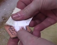
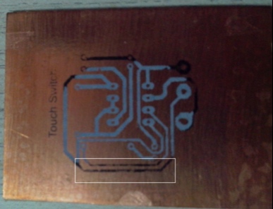
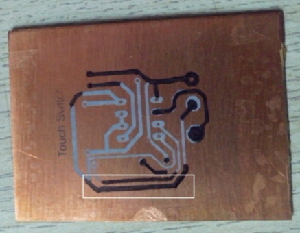
In some cases, when removing the paper, some of the tracks get fainted. In the figure below, you can see that the track is light in color, hence we can use a black marker to darken it as shown.
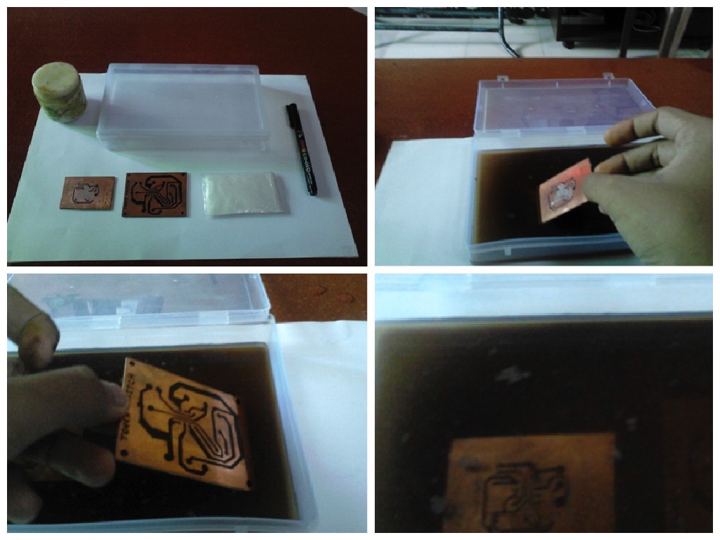
STEP 5: Etch the Plate
You need to be really careful while performing this step.
- First, put on rubber or plastic gloves.
- Place some newspaper on the bottom so the etching solution does not spoil your floor.
- Take a plastic box and fill it up with some water.
- Dissolve 2-3 teaspoons of ferric chloride power in the water.
- Dip the PCB into the etching solution (Ferric chloride solution, FeCl3) for approximately 30 mins.
- The FeCl3 reacts with the unmasked copper and removes the unwanted copper from the PCB.
- This process is called Etching. Use pliers to take out the PCB and check if the entire unmasked area has been etched or not. In case it is not etched, leave it in the solution for some more time.
STEP 6: Cleaning, Disposal, and the Final Touches for the Circuit Board
Be careful while disposing of the etching solution, it’s toxic to fish and other water-based organisms! Don’t even think about pouring it in the sink when you are done, it is ILLEGAL and might damage your pipes (hehe, who knew you could get arrested while making a PCB?!). Instead, dilute the etching solution and then throw it away somewhere safe.
A few drops of thinner (nail polish remover works well) on a pinch of cotton wool will remove completely the toner/ink on the plate, exposing the copper surface. Rinse carefully and dry with a clean cloth or kitchen paper. Trim to final size and smoothen edges with sandpaper.
Now, drill holes using a PCB driller like this PCB driller and solder all your cool components to the board. If you want that traditional green PCB look, apply solder resistant paint on top PCB lacquer. And finally, your super cool circuit board will be ready!