Learn the basics of PCBs and the information needed to get started designing your first PCB.
Learn the basics of PCBs (printed circuit boards) and learn the information needed to get started designing your first PCB. In this tutorial, I'll explain what PCBs are, the different types, what they're made of, how they're manufactured, and the software used to make them.
What Is a PCB?
- PCBs are the backbone of electronic devices.
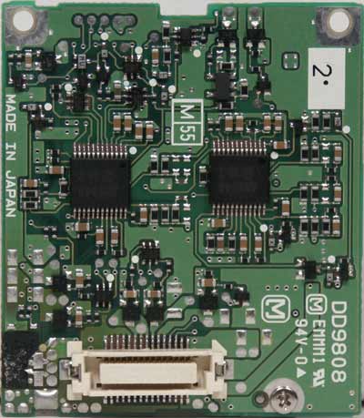
- A PCB is a non-conductive board that holds all electronic components through a circuit embossed over it.
- PCBs are built to last for a wide range of industrial, commercial, and domestic applications.
- They can be customized to any specifications to users’ requirements.
Basic History of PCBs
- PCBs were first developed during World War II.
- The revolutionary invention was made by an Austrian engineer, Paul Eisler.
- Since 1929, PCBs have been mass produced for commercial applications.
- They were first used in transformers and capacitors.
PCB Types
- Single sided: Base material (rigid laminate with a woven glass epoxy base material) clad with copper on one side.
- Double sided: The assembly encompasses a base material with copper on both sides.
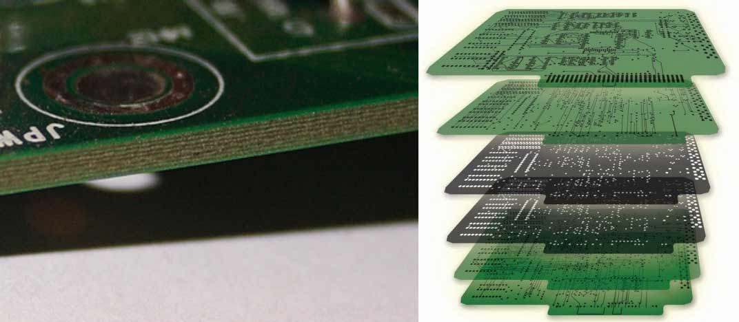
- Multi-layered: Encompasses several layers of substrates. Each layer is separated by insulation.
Board Styles
- Rigid: Solid construction.
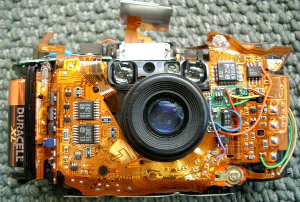
- Flex: Flexible circuits.
- Rigid-flex: Multiple layers of flexible substrates attached to one or more rigid boards.
- Hybrid: Very small circuit. Can be integrated as part of a larger circuit.
Parts of a PCB
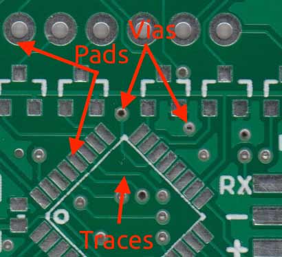
- Pads: Location where components are connected/soldered to.
- Traces: Connect pads together.
- Vias: Conduct the electrical connection between layers of the PCB.
- Top metal layer: The layer where most of the components are assembled. There are few traces in the top metal layer.
- Bottom metal layer: Has more traces—but fewer components than the top metal layer.
Components
The actual devices on the board. PCB components can be categorized as active and passive.
Active Components
- Diode: Allows current to flow in one direction.
- Transistor: Amplifies and switches electrical power and electronic signals.
Integrated circuits (ICs): Responsible for several signal processing functions.
Passive Components
- Capacitor – Stores and discharges electricity.
- Resistor – Limits the power of the electrical current.
- Inductor – Creates a magnetic field.
PCB Package Types
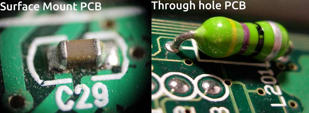
PCB components can be mounted onto the board in two ways:
- Surface mount: PCB components are mounted directly onto the board.
- Through-hole: Components with leads are inserted through mounting holes, hence the name "through-hole".
PCB Manufacturing/Assembly Steps
- Base material preparation: Clean the laminate, containing the copper foil.
- Cutting the base material: Post the cleaning process, cut the laminate to required specifications.
- Apply adhesive on the laminate: Choose between epoxy or acrylic adhesives to get the job done.
- Generate circuit pattern: Desired circuit patterns can be generated by screen printing or photo imaging.
- Etch the circuit pattern: Etch the copper laminate containing the circuit pattern.
- Drilling: Drill holes, pads, and vias by using high-speed drilling tools.
- Through-hole plating: Deposit the holes with copper and must be chemically plated.
- Apply cover lay: Protect the top and bottom side of the board by applying suitable cover lay.
- Cutting flex: Cut individual flex from the production panel.
- Cleaning: Clean flux residues that are left behind during the manufacturing process. Use water solution or active cleaning agents to get the job done.
- Testing: This Includes Automated Optical Inspection (AOI), flying probe test, functional test, and burn-in test.
- Rework: Rework may be done on the PCB in case of missing components, component replacement, trace or pad repair, and cuts and jumps.
PCB Material Options
When it comes to manufacturing PCBs, there are several material options available:
Substrate Material
- Epoxy imprinted fiberglass
- Polyester (PET)
- Polyimide
Conductor Material
- Electro-deposited copper foil
- Rolled copper foil
Adhesives
- Polyimide adhesives
- Polyester adhesives
- Acrylic adhesives
- Epoxies
Protective Coating
- Polyamide adhesives
- Cover lays: Polyester or polyamide is combined with a suitable adhesive.
- Cover coat: A thin coating of liquid acrylate epoxy and acrylate polyurethane.
EAGLE
- Stands for Easily Applicable Graphic Layout Editor.
- Flexible, expandable and scriptable EDA application with schematic capture editor, PCB layout editor, and auto-router.
- The latest version is 6.1, and minimum requirements are MAC OS X 10.6, Linux 2.6, or Windows XP.
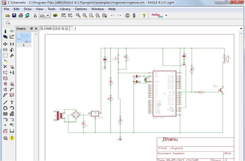
- Schematic drawing on EAGLE:
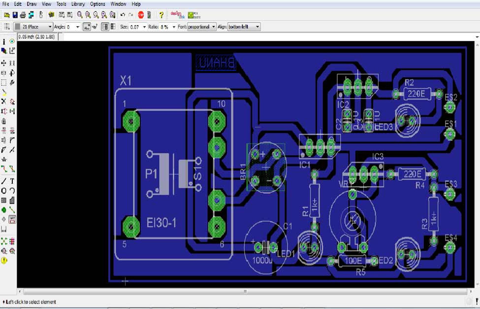
- Board design and routing on EAGLE:
I hope this PCB basics tutorial helped you get a better understanding of PCBs. You should now know enough now to start designing your own. Stay tuned to the follow-up tutorial for designing PCBs on EAGLE!
Further Reading

