Learn all about Tab-Route Panels and how to go about them in Eagle in the last part of this series on PCBs!
So far in this article series, we’ve learned about what PCB panelization is and why it is advantageous for manufacturing PCBs at scale versus manufacturing PCBs individually. We learned about the two main methods of creating the removable connections between the individual PCBs in a panel: V-groove and tab-route. In the previous article, we learned how to create a V-groove panel in Autodesk EAGLE. Now, in this final article, we will learn how to create a tab-route panel in EAGLE.
Creating tab-route panels is more complex than V-groove panels. Tab-route panels simply have more complex geometry compared with V-groove panels. Rather than simply running a saw in a straight line across the board, tab-route panels use more complex CNC-routed slots between boards, with perforated tabs between PCBs. Tab-routed panels also require a margin around the entire panel that allows machinery to securely hold the panel.
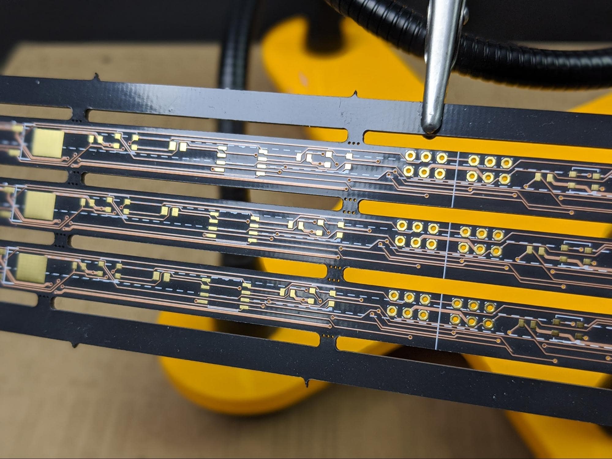
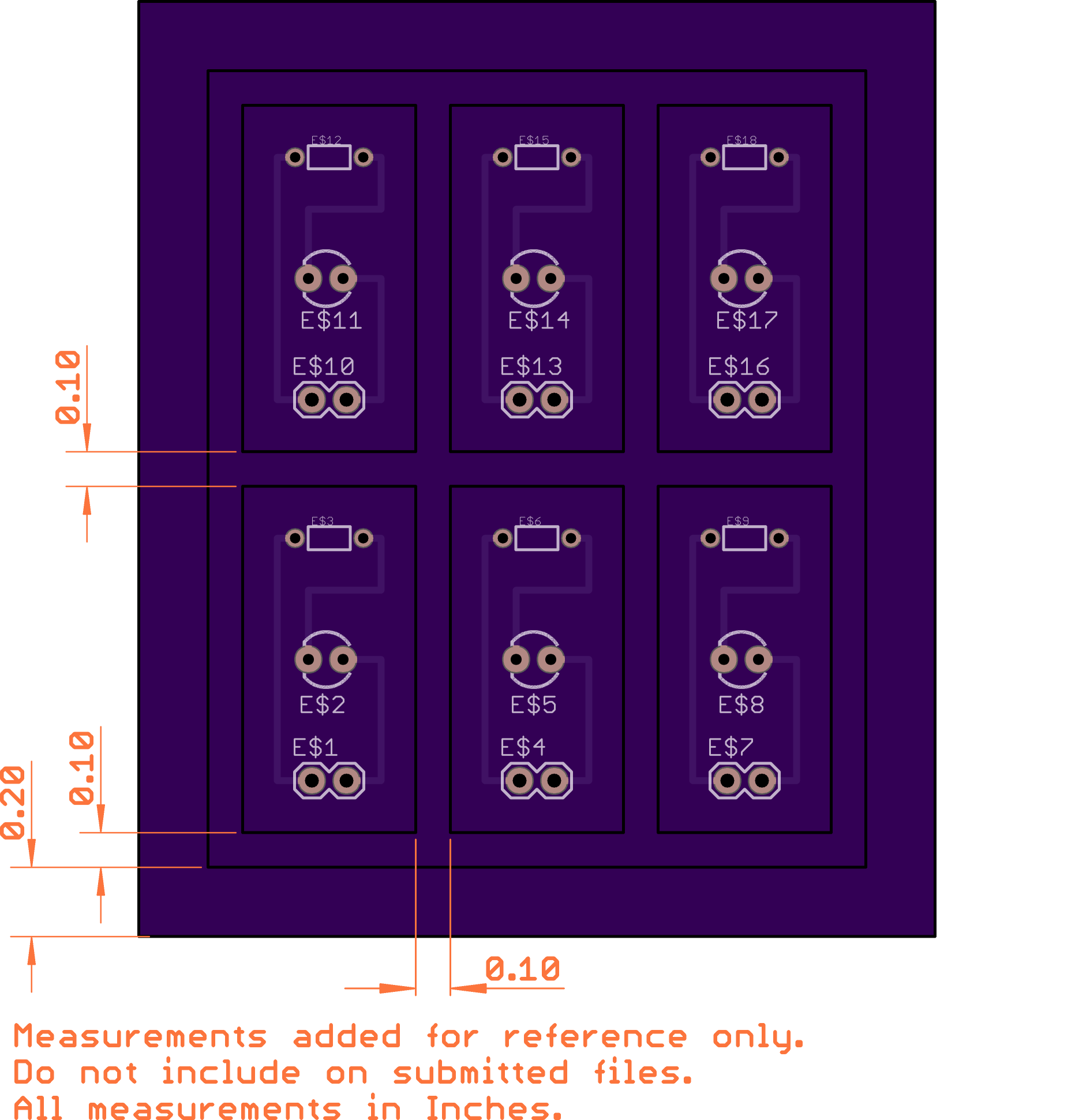
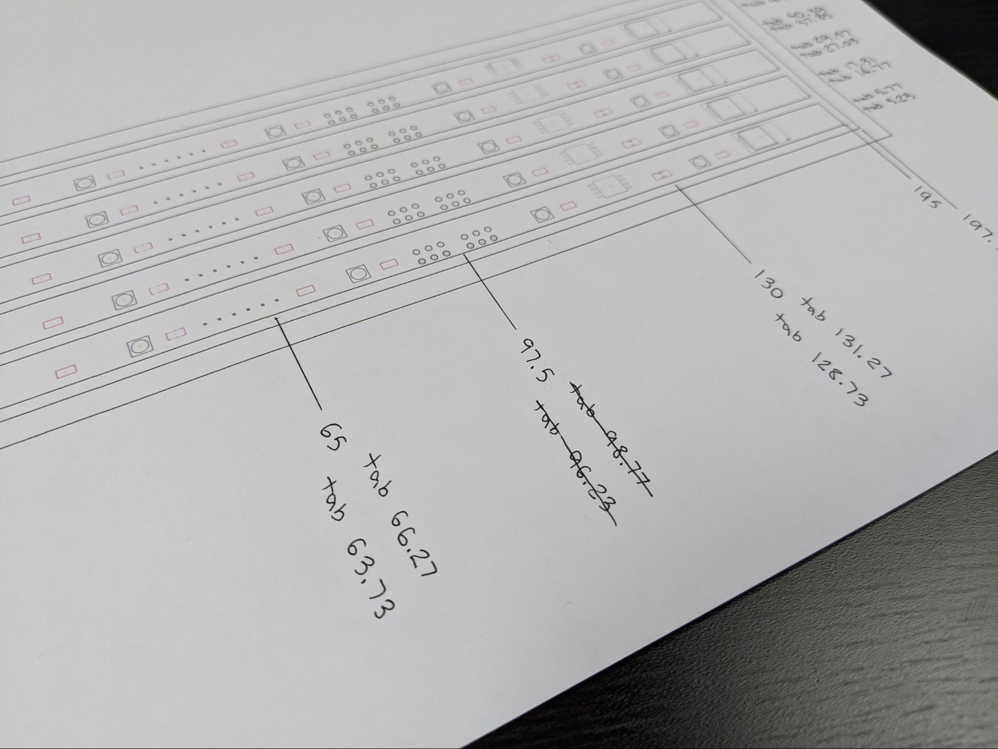
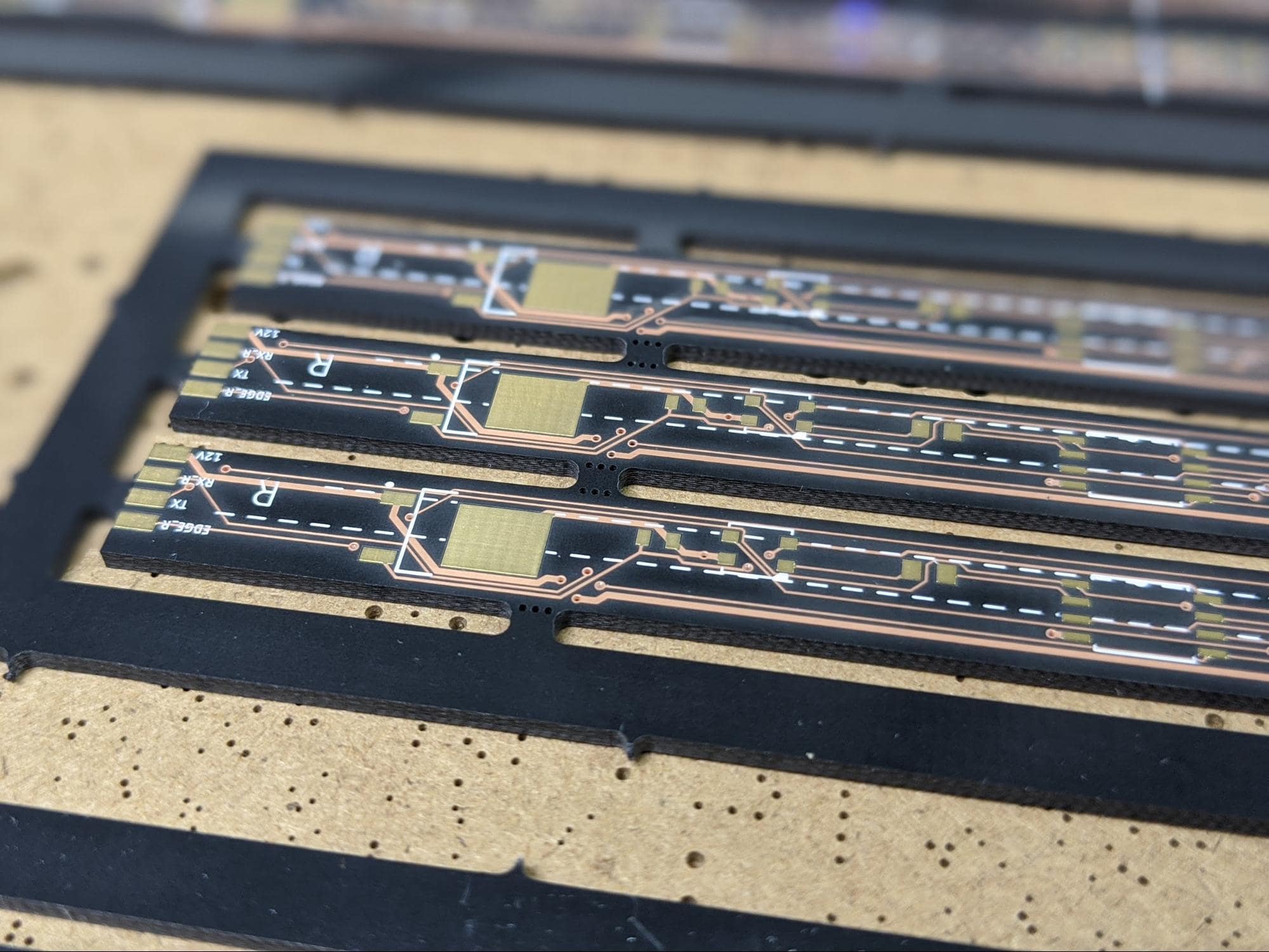
In this photo, you can see the perforated tabs separating the individual PCBs.
These geometric requirements mean you need to pay close attention to the design specifications from your PCB manufacturer. In this tutorial, we will be designing a panel for OSH Park because they have the best documentation around.
How to Create Tab-Route Panels in EAGLE
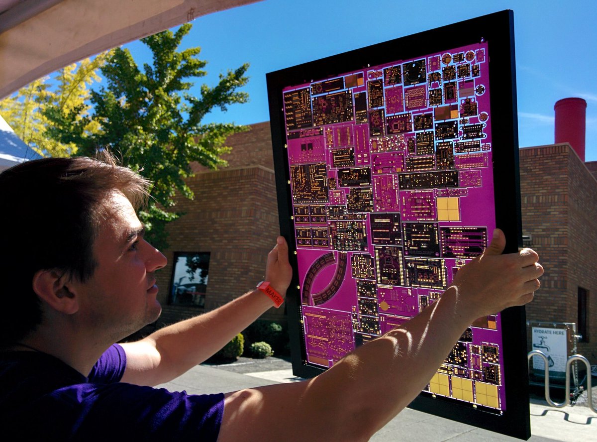
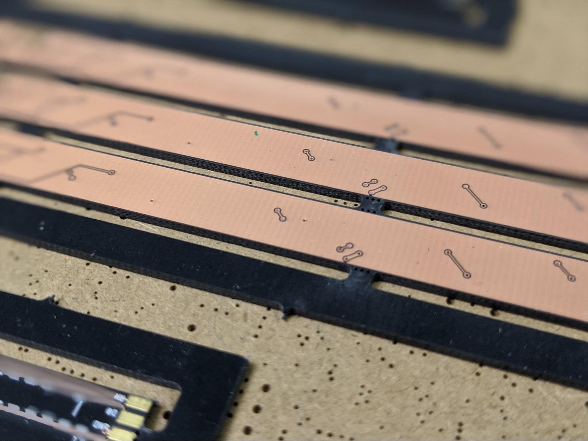
This is a finished panel from OSH Park. You can see the perforated tabs separating the individual PCBs and the frame around the entire panel.
Step 1: Download and Set Up the SparkFun Panelized ULP
We begin the process of creating a tab-routed panel the same way we started designing the V-groove panel in the previous section: by using a ULP from SparkFun to make copies of the PCB without messing up the part designators.
So, download the entire SparkFun EAGLE Settings repository from GitHub. Then, move the SparkFun-Panelizer.ulp file from the \ulp directory in the repository into the Eagle \ulp directory (typically \Documents\eagle\ulps). Move all the DRU files from the \dru directory in the repository into the \design rules directory in your EAGLE installation. This is typically located in \Documents\eagle\design rules.
Step 2: Run the ULP to Create Board Copies
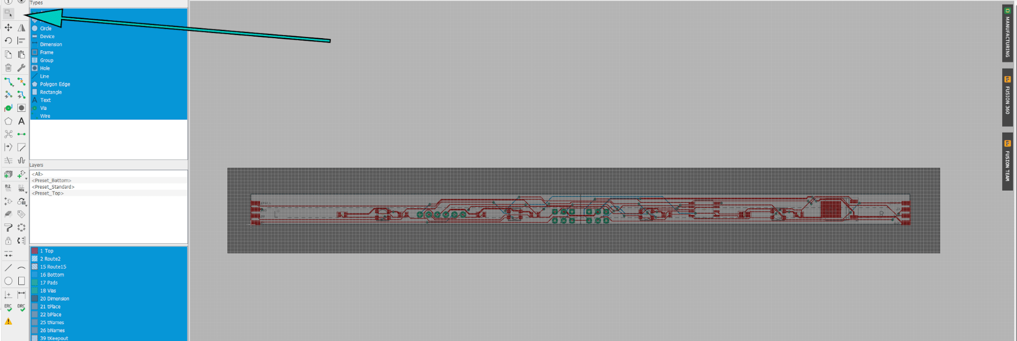
Next we use the SparkFun Panelizer ULP to create copies of the PCB. Start by using the Group tool to select everything in your design; make sure all the layers you need in your panel are visible.
Use the Group tool to select the entire deisgn.
Then, using the Copy tool, right-click anywhere and select Copy: Group. This will place a copy of your board into the clipboard that the ULP will use to create a panel. Do not paste the board though, just copy it.
Use the Copy tool to right-click and select Copy: Group.
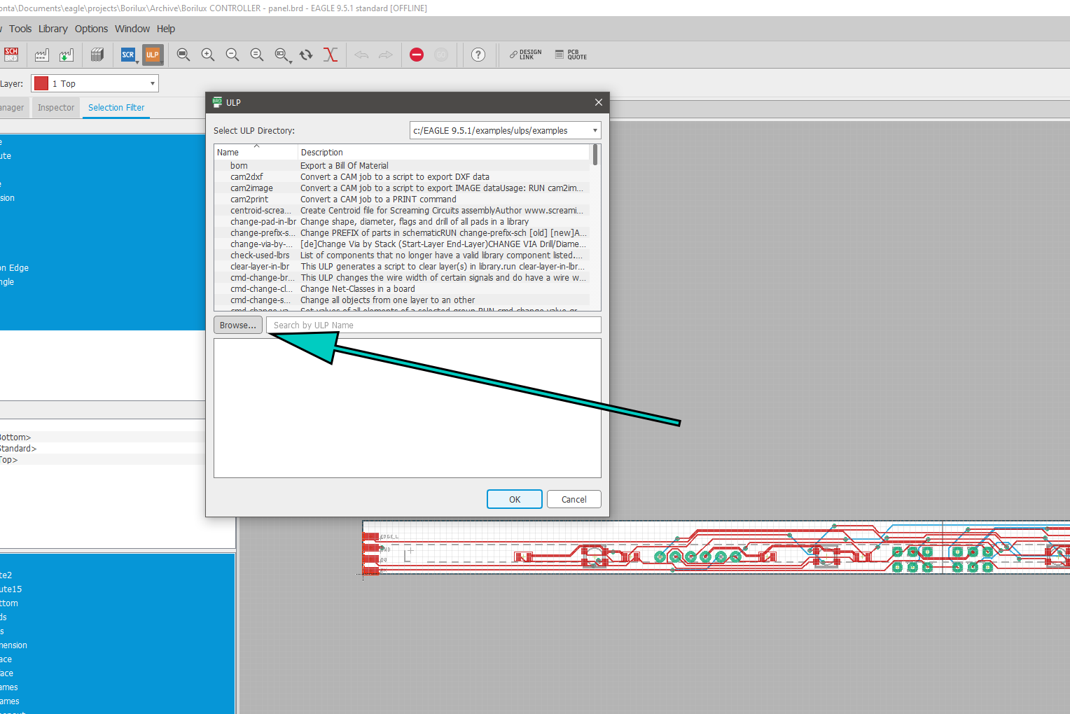
Click the ULP button in the toolbar and, from the dialog box, click the Browse button. Then, find the SparkFun-Panelizer.ulp you placed in your EAGLE installation directory earlier.
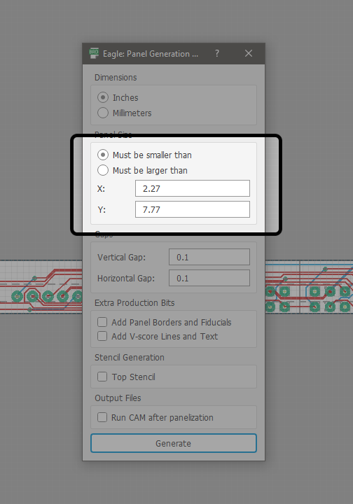
There are a few settings we will adjust in the dialog box for the ULP. First we need to figure out the overall dimensions of the panel. For the X value, multiply the width of your board and add 0.1 inch for each board. Similarly, for the Y value, multiply the height of your board and add 0.1in for each board.
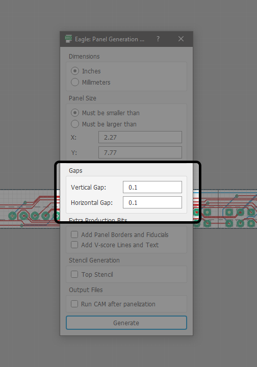
The reason we add 0.1 inch (2.54mm) for each board is to create a space between copies of the board in which we will create tabs to hold the boards together. Therefore, the next parameter to adjust in the dialog box for the SparkFun Panelizer ULP is the vertical and horizontal spacing. Set both of these to 0.1 inch.
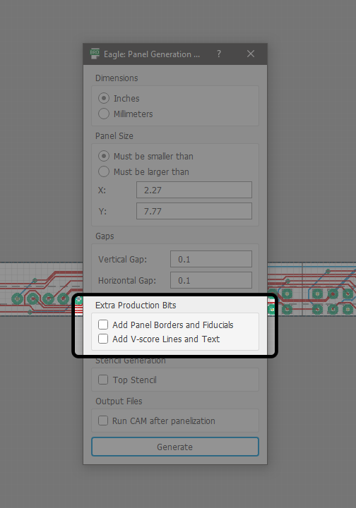
Lastly, because we will be using tab-route panelization in this tutorial, we will not have the ULP create V-groove lines in the design. Therefore, in the Extra Production Bits section, deselect the Add V-score Lines and Text option.
Finally, press the Generate button and the ULP will create copies of your board, spaced apart by 0.1 inch.
The SparkFun_Panelizer ULP will create an array of PCBs spaced apart by 0.1 inch
Step 3: Create the Frame
With the array of PCBs created, the next step is to create a frame around the entire set of PCBs. The frame is simply an area of blank FR4 around the entire design. The frame allows your PCB manufacturer to fasten the PCB array to the machinery needed to route the board and assemble it. Like with the spacing between boards and the recommended geometry for the tabs (more on that in the next step) it is important to carefully read your manufacturer's documentation so you know the requirements for the frame.
For OSH Park, the frame must be at least 0.2 inch (5.08mm) wide around the entire design. The frame must also be free of any design elements or text or dimensions. Also, just like the space between the individual PCBs, there must be a 0.1 inch space between the boards and the inside edge of the frame.
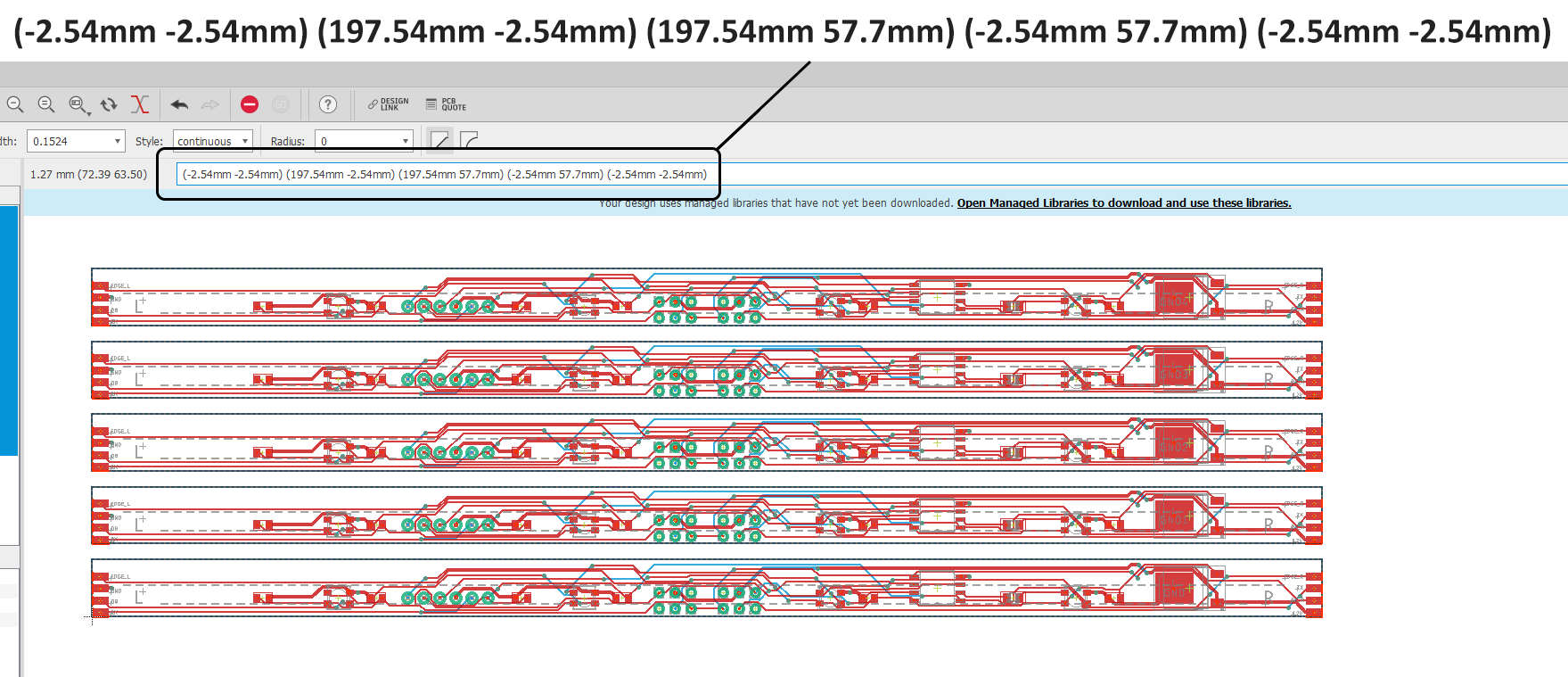
To draw the frame, use the Line tool on the dimension later. We will start with the inner edge of the frame, which is 0.1 inch away from the PCBs. Find the coordinates for the sides of the frame by subtracting 0.1 inch from the left side and bottom side of the PCB array, and adding 0.1 inch to the right and top sides of the array. Use the command entry line at the top of the window to input the coordinates of each corner of the rectangular frame.
A command with the coordinates for all four corners of the inner side of the frame can be used to create a rectangle to represent the inner side of the frame.
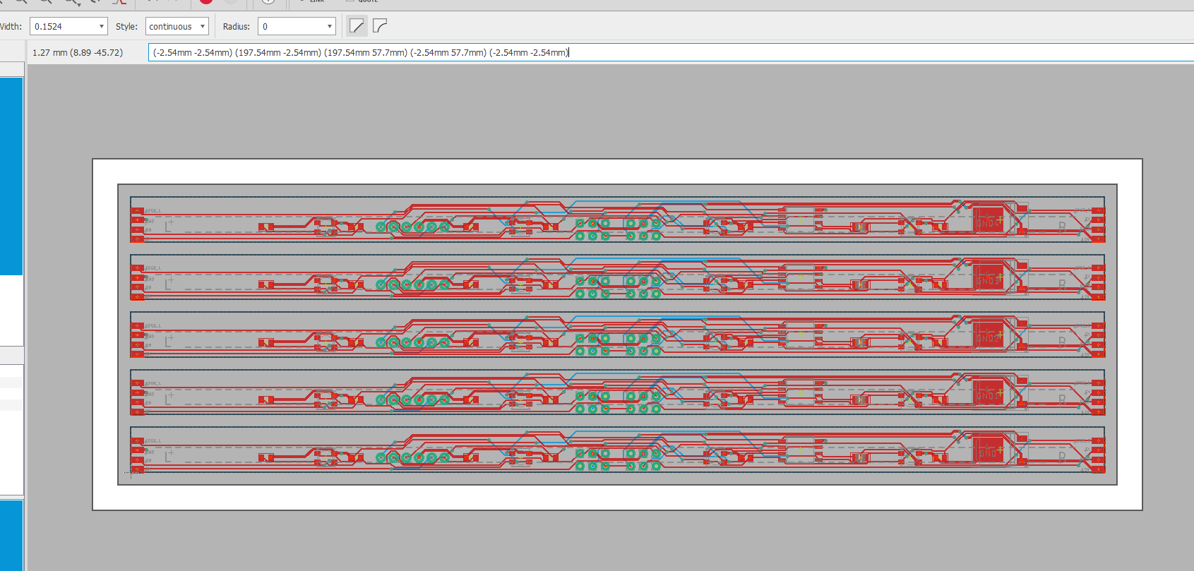
Then, use the same procedure to find the outside edge of the frame; this time add or subtract 0.3 inch from the sides of the PCB array to account for the 0.1 inch gap and the 0.2 inch width of the frame.
Using a similar command, create the outer edge of the frame enclosing the design
Step 4: Create Tabs
Now that we have an array of PCBs, and a frame around them, we can create the small tabs that will hold the PCBs together and hold the PCBs to the frame while the PCBs are being made and assembled.
Note: If you are using OSH Park, you can just skip this step and the next one. OSH Park will automatically create tabs in your design. You can just upload your Eagle BRD file with a PCB array and a frame, and the tabs will be automatically inserted.
The geometry of the tabs are another design element that you need to make sure to verify with your PCB manufacturer. For OSH Park, the tabs should be 0.1 inch wide. In general, you will want to place at least one tab on each side of the board to provide enough strength to hold the panel together during the manufacturing and assembly processes. If you have a relatively long PCB, like the one in this example that is about 200mm long, you may wish to place two tabs on the long sides for added rigidity.
Creating the tabs involves a bit of simple geometry and math. I find it easiest to print a copy of the PCB array and plot the coordinates for the tabs so they can be entered easily.
Find the center point of each side of your PCB (or ⅓ of the width of you are placing two tabs on a side). Then, add 0.05 inch (1.27mm) from the center point to find one side of the tab and subtract 0.05 inch to find the other side of the tab. From each of these points draw a line 0.1 inch (2.54mm) long so that it meets the adjacent PCB or the frame around the array.
Horizontal Tabs
PCB Copy | Center | Tab Bottom Line | Tab Top Line |
|---|
1 | (2.54mm, 4.5mm) | (0, 3.23mm) to (2.54mm 3.23mm) | (0, 5.77mm) to (2.54mm 5.77mm) |
2 | (2.54mm, 16.04mm) | (0, 14.77mm) to (2.54mm, 14.77mm)
| (0, 17.31mm) to (2.54mm, 17.31mm)
|
3 | (2.54mm, 28.3mm) | (0, 26.31mm) to (2.54mm, 26.31mm)
| (0, 28.85mm) to (2.54mm, 28.85mm) |
4 | (2.54mm, 39.12mm) | (0, 37.85mm) to (2.54mm, 37.85mm)
| (0, 40.39mm) to (2.54mm, 40.39mm) |
5 | (2.54mm, 50.66mm) | (0, 49.39mm) to (2.54mm, 49.39mm)
| (0, 51.93mm) to (2.54mm, 51.93mm)
|
This table shows an example of finding the coordinates for the tabs on one side of the PCB array by plotting lines 1.27mm above and below the center point of the PCB
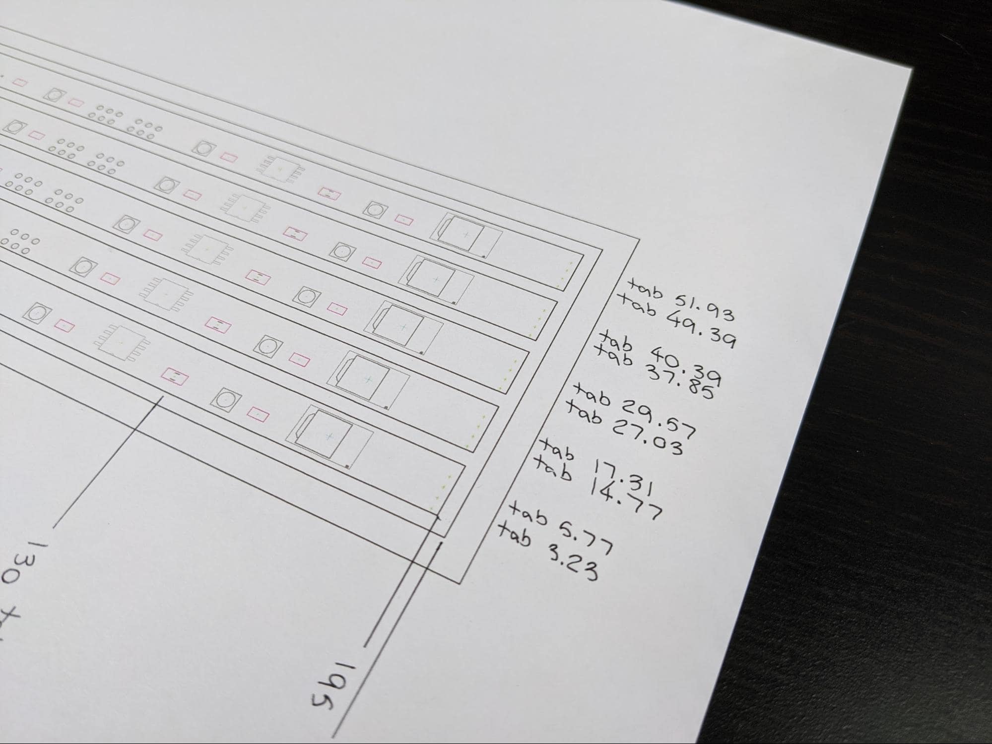
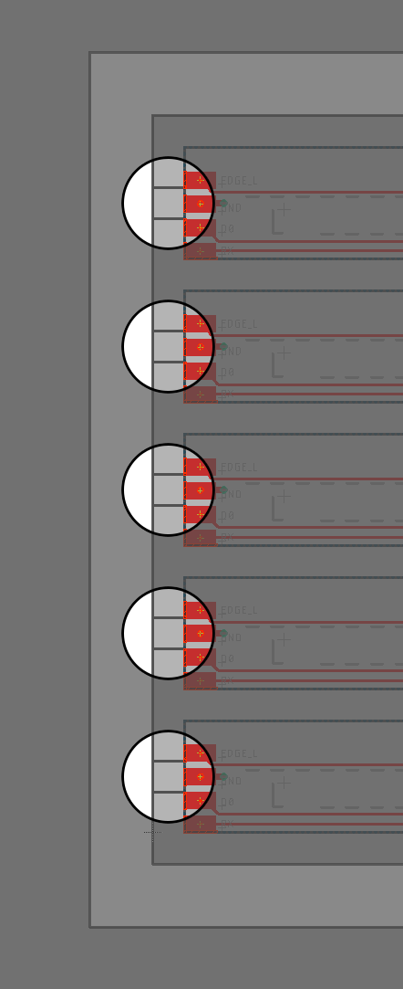
Using the coordinates in the table above, tabs can be created for the left side of each PCB, connecting them to the frame.
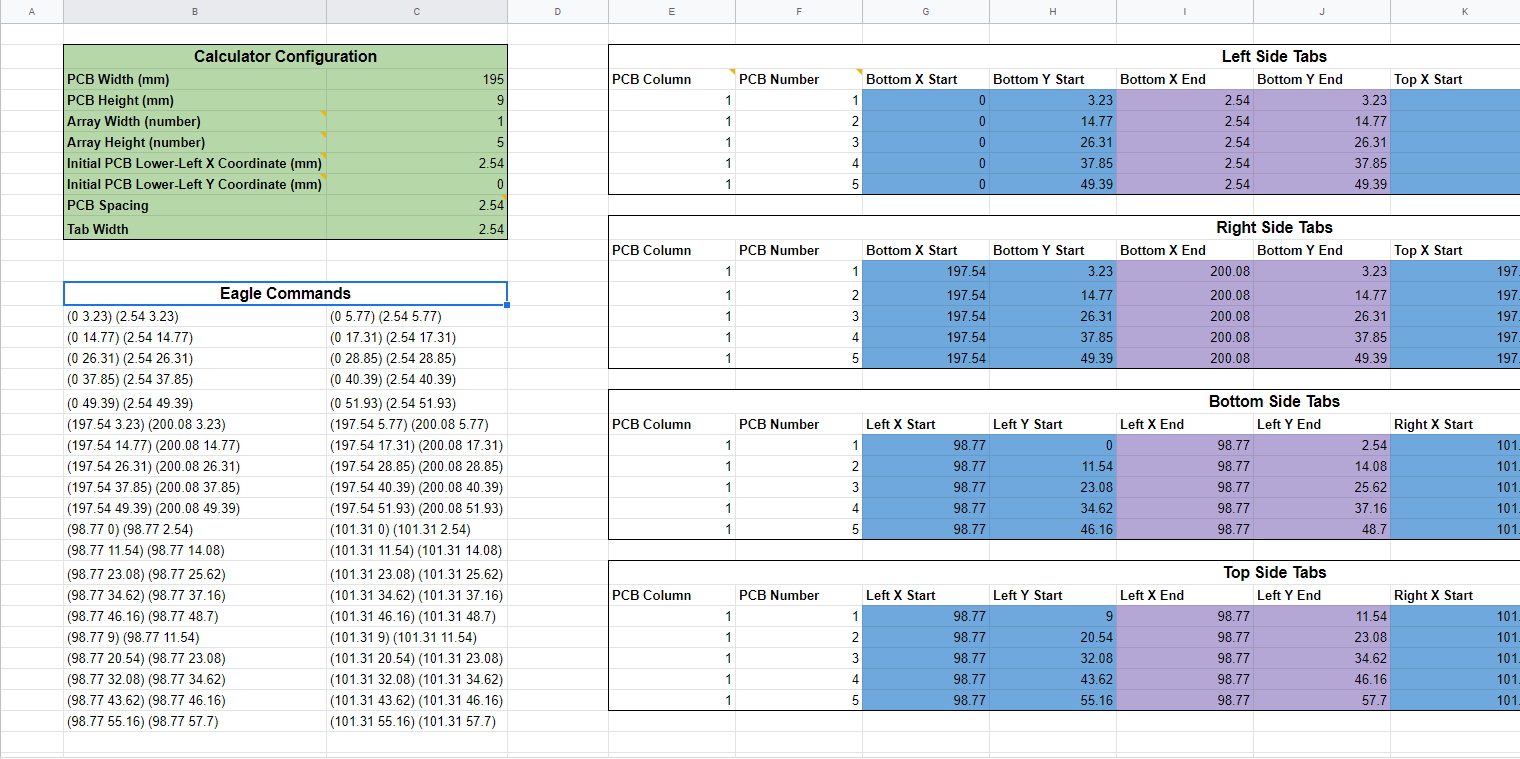
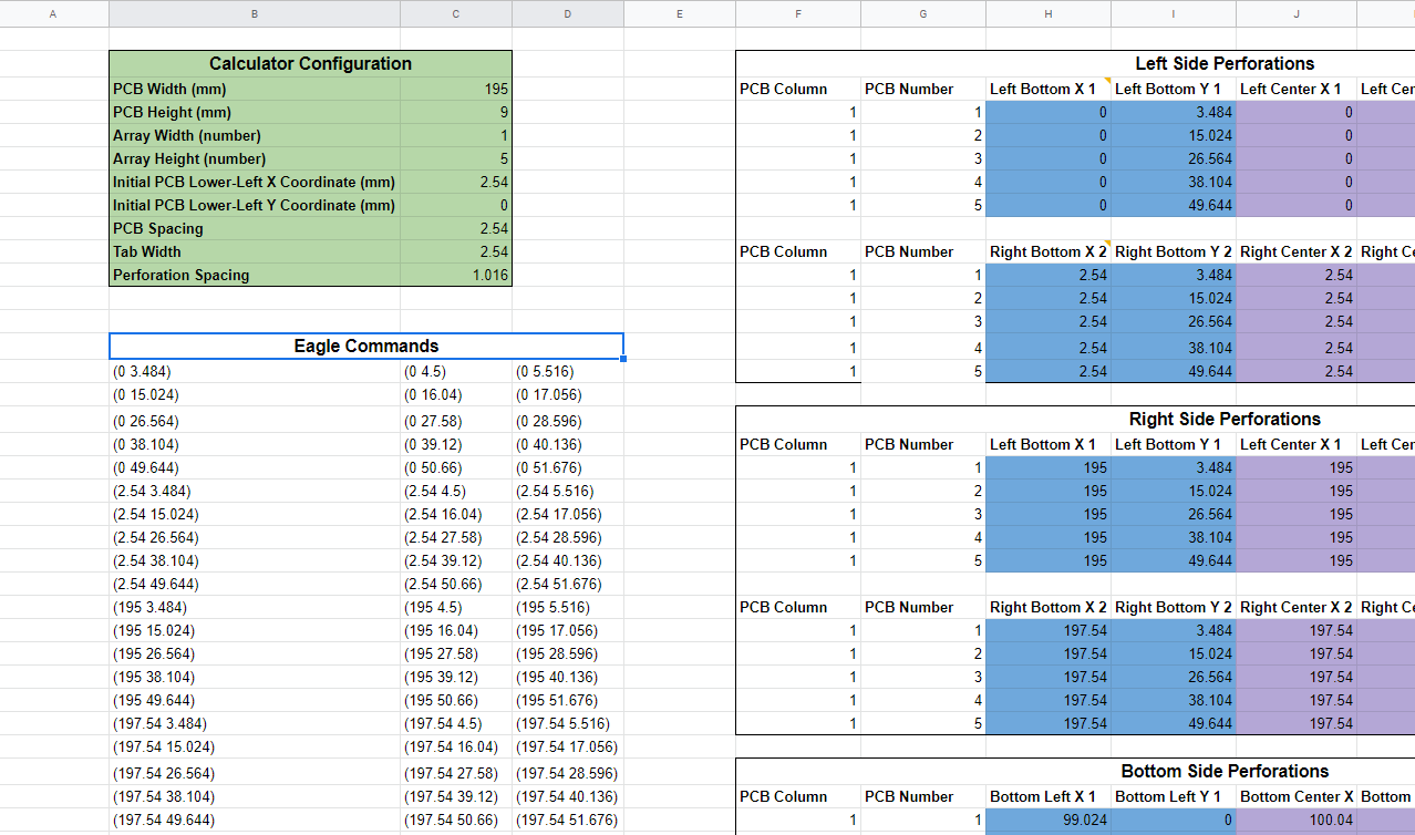
To make the process a bit easier, especially if you are designing a number of panels, I also created a spreadsheet in Google Drive to calculate the locations of your tabs, placing one tab on each side of each PCB.
To use the calculator, input the width and height of your individual PCBs, and how many copies of your PCB are in the vertical direction. The spreadsheet will return a list of tab coordinates containing the start and end coordinates for the lines that make up each side of the tabs.
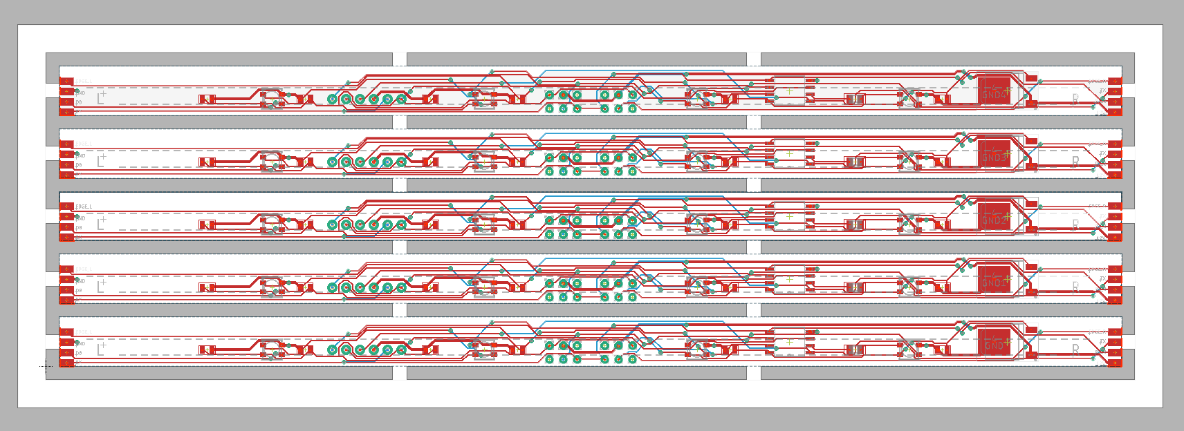
By the time you are done drawing all the lines making up the tabs, you will be left with an array of PCBs, surrounded by a frame, with the frame and all the PCBs connected by small tabs.
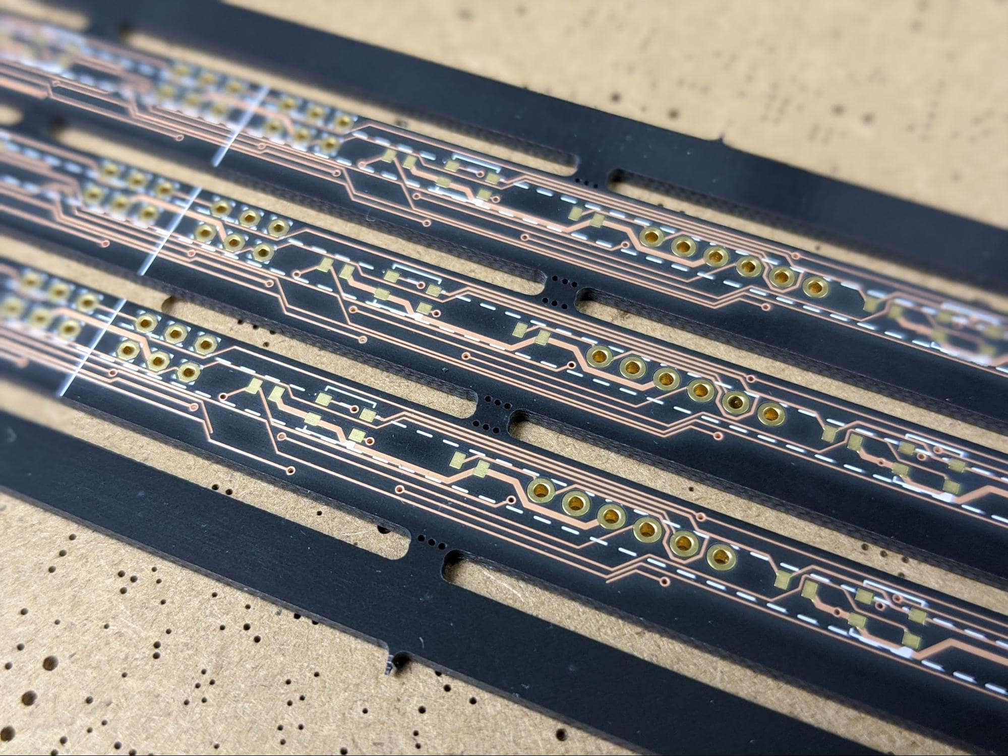
In this image, you can see the tabs joining together all the PCBs and connecting the PCB array to the frame.
Step 5: Create Perforations
Even for little tabs only 0.1 inch wide, the FR4 material from which PCBs are made is quite strong. In order to reduce the force required to depanel the boards, we will place small holes at the base of each tab. This perforation makes it much easier to break the PCBs apart.
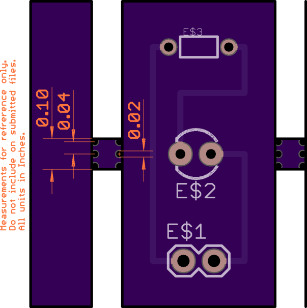
Just like creating the tabs themselves, placing the perforations will require some math. We will again be using documentation from OSH Park. At the base of each tab, on both sides of each tab, we will draw a row of three holes. Depending upon how strong you'd like the tabs to be, the holes can be the standard size of 0.02 inch or they can be increased in size to 0.025 inch.
So, one hole goes in the center of the tab, with the other two spaced 0.04 inch (1.016mm) on each side. If you already have the center points of each PCB written down from creating the tabs in the previous step, simply add/subtract 0.04 inch (1.016mm) to find the positions for the flanking holes.
Alternatively, the spreadsheet used in the previous step to calculate the coordinates of the tabs has a second sheet that can be used to calculate the positions of the holes. This sheet uses the configuration information from the first sheet to perform its calculations.
Step 6: Generate and Verify Gerber Files
Now that all the tabs and all the holes are in place, it is time to send the files to get manufactured. If you are using OSH Park, the process is extremely easy because you can simply upload the BRD file containing your panel design. Otherwise, most other PCB manufacturers use Gerber files. Gerber files are a set of files, each containing information about different parts of your design.
To generate Gerber files from your EAGLE design, use the CAM Processor button in the toolbar.
A Recap on Tab-route Panelization
Tab-route panelization is useful for panels in which the individual PCBs cannot be separated by simple straight lines (in which case V-groove panelization is an easier method). This may be the case because the boards in the panel have complex, or at least non-rectangular shapes. This may also be the case in panels made from several different board designs, as is the case for batch PCB services like OSH Park.
OSH Park uses tab-route panelization to create large panels made from PCBs submitted by multiple customers.
While tab-route panelization is more complex than V-groove panelization, it is also more versatile. As long as care is taken to follow the panel specifications of your PCB manufacturer, tab-route panelization can be used to manufacture essentially any board shape.
