Keep your projects from over heating with this helpful guide on different techniques fo better heat management!
No PCB can be properly designed without thoughtful consideration of how the heat it generates will dissipate. Without a plan in place, components may heat up rapidly, increasing their risk of failure. All sorts of components are susceptible to heat damage — microcontrollers, amplifiers, passive components (commonly, resistors), and others.
In this article, I’ll discuss how heat transfer works and different ways you can design your PCBs to protect them against heat-related damage.
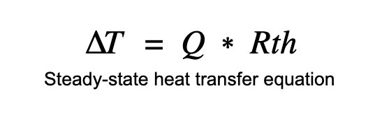
The Formula for Heat Transfer
Heat transfer is largely analogous to electricity, with the formula for steady-state heat transfer closely resembling Ohm’s law.
A difference in temperature (∆T) is equal to the amount of heat generated (Q) times the thermal resistance (Rth) of the medium. Sure sounds a lot like a V = IR, a difference in voltage equal to current times resistance!
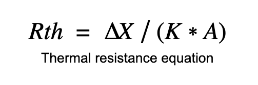
The Formula for Thermal Resistance
The thermal resistance of a medium is equal to its length (∆X), which is divided by its cross-sectional area (A) times the thermal conductivity of the material (K). This also sounds a lot like electrical resistance (R = ρL/A, resistivity times length divided by cross-sectional area).
It may not always be practical or important to plug numbers into these equations, but it is important to consider which components may be generating the most heat and how to keep them cool and operational.
Utilizing Heatsinks for Heat Dissipation
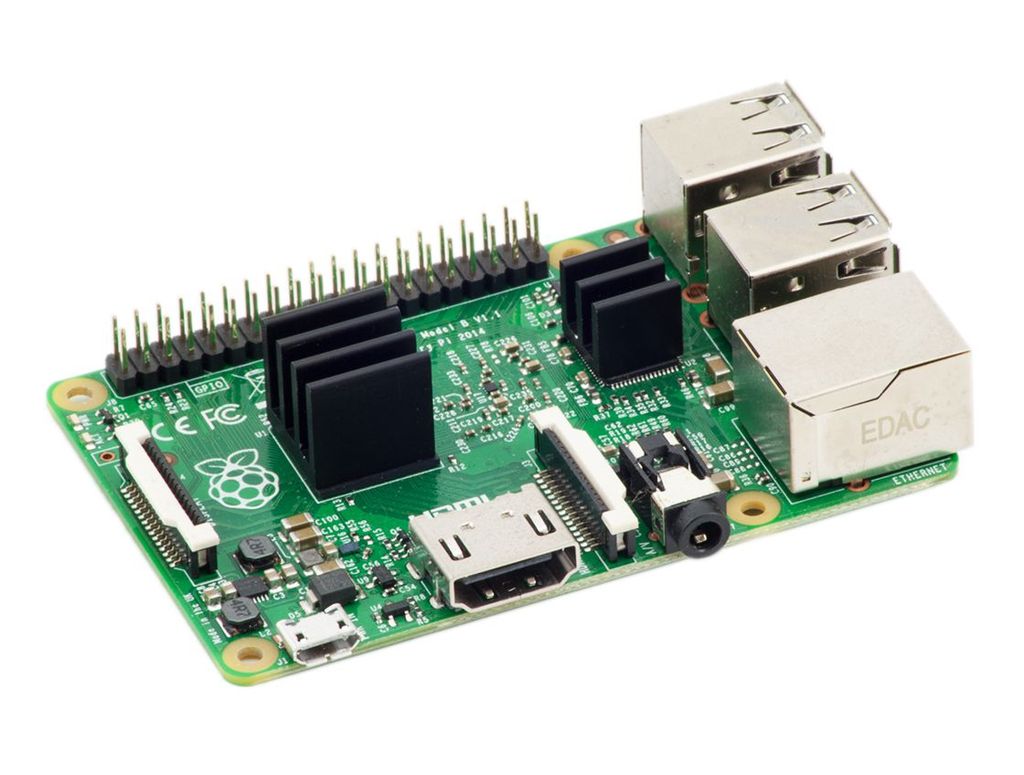
Components such as microprocessors, voltage regulators, and power amplifiers (amongst many others) often use heatsinks to help dissipate the heat they generate and stay cool. Often, it’s as simple as a piece of metal attached to the device that helps transfer the heat from the device to the air. They work by increasing the amount of surface area exposed to air, which lowers the thermal resistance.
Heatsinks on a Raspberry Pi. In this case, they’re on the processor and Ethernet ICs. Image courtesy of The Pi Hut
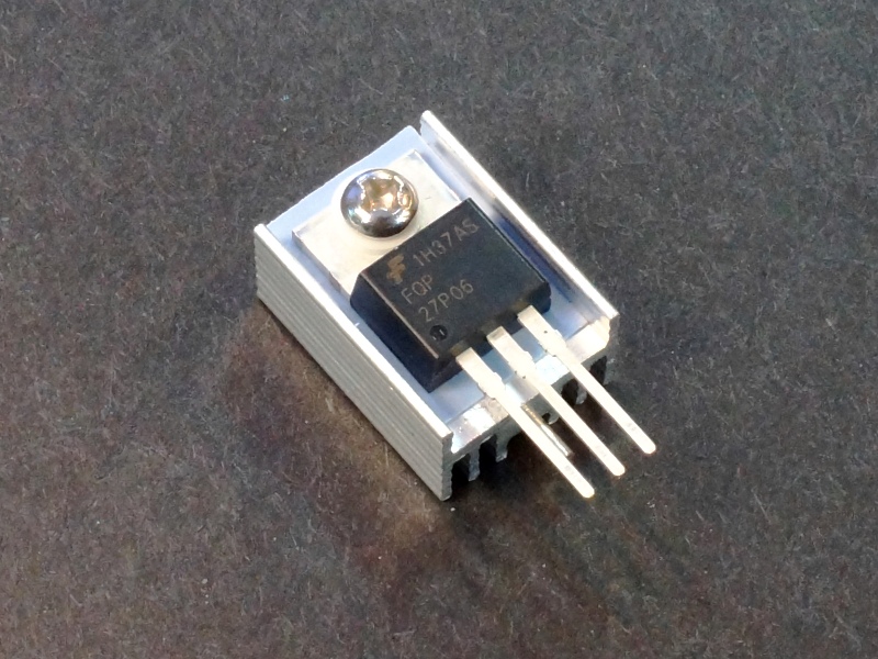
Off-the-shelf heatsinks are available for many standard component packages, such as for the TO-220 shown. That heatsink can work for anything using that package, whether it be a MOSFET, linear regulator, amplifier, or anything else. The heatsink is attached to the component with either thermal tape or a type of thermal paste/glue — a material that helps the heatsink make full contact with the component and maximize the heat transferred between them.
PCB Design Techniques for Heat Transfer
Copper pours on a PCB are an excellent way to help a device perform better, electrically and thermally. Ground pours (filling all unused space on the board with metal connected to ground) allow any component on the PCB to easily connect to ground. Power planes, or power polygons, allow more current to be delivered to devices than is possible through just a trace.
Power planes or polygons aren’t always possible, especially on two-layer boards. Power traces carry more current than signal traces, so we route them wider. This decreases their thermal (and electrical) resistivity, allowing them to dissipate heat easier, stay cooler, and not burn up. Many current trace thickness calculators are available online, and should be consulted during a design.
A design technique often coupled with copper pours is to include thermal vias. Components on one side of a PCB may benefit from connecting to a power polygon, or ground pour, on the other side of the board, or on an internal layer. Thermal vias act as an electrical and heat pathway between the component and that large area of copper.
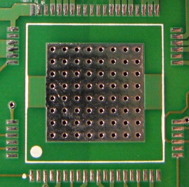
The packages of many surface mount ICs include a thermal pad under the device (also called an exposed pad). This is a large metal pad, usually electrically connected to ground, intended to provide mechanical support and a pathway for heat dissipation for the chip. Many datasheets will recommend the layout include thermal vias in that pad. It is not recommended to place vias in small SMD pads (it can cause manufacturing problems in automated soldering), but it’s common to do so in large under-device thermal pads.
Footprint for a large IC, with a thermal relief pad fitted with thermal vias. Image courtesy of Screaming Circuits
Thermal Relief Connections
Thermal relief connections are one of the few examples of techniques to increase heat in the PCB.
When soldering, the objective is to heat a joint up enough to quickly melt solder onto it and create a strong electrical (and to a lesser extent, mechanical) connection. A footprint pad that is exceptionally thermally treated, such as a ground pin connected directly to several ground planes, may be difficult to solder to. The heat is dissipated more quickly than it can accumulate and raise the temperature. For this reason, it is sometimes helpful to add thermal relief to the copper pour’s connection settings in your CAD tool.
Thermal relief connections don’t directly connect the component pad to the copper pour. Instead, they connect using thin tracks. This increases the thermal resistance between the pad and the pour. The heat from a soldering iron, reflow oven, or hot air gun will cause the temperature of the pad to rise faster, since the heat cannot dissipate as quickly. This makes soldering much faster and easier.