Once your circuit has been tested and and you see that it works, learn how to translate your design on a PCB!
After developing a breadboard prototype, the next stage in developing electronics for a product is to translate the design onto a PCB.
After creating a schematic design using ECAD software, like Autodesk Eagle, there are a number of different ways to prototype your PCB. These range from prototype-specific techniques to the same technologies used for electronics manufacturing, just at a smaller scale.
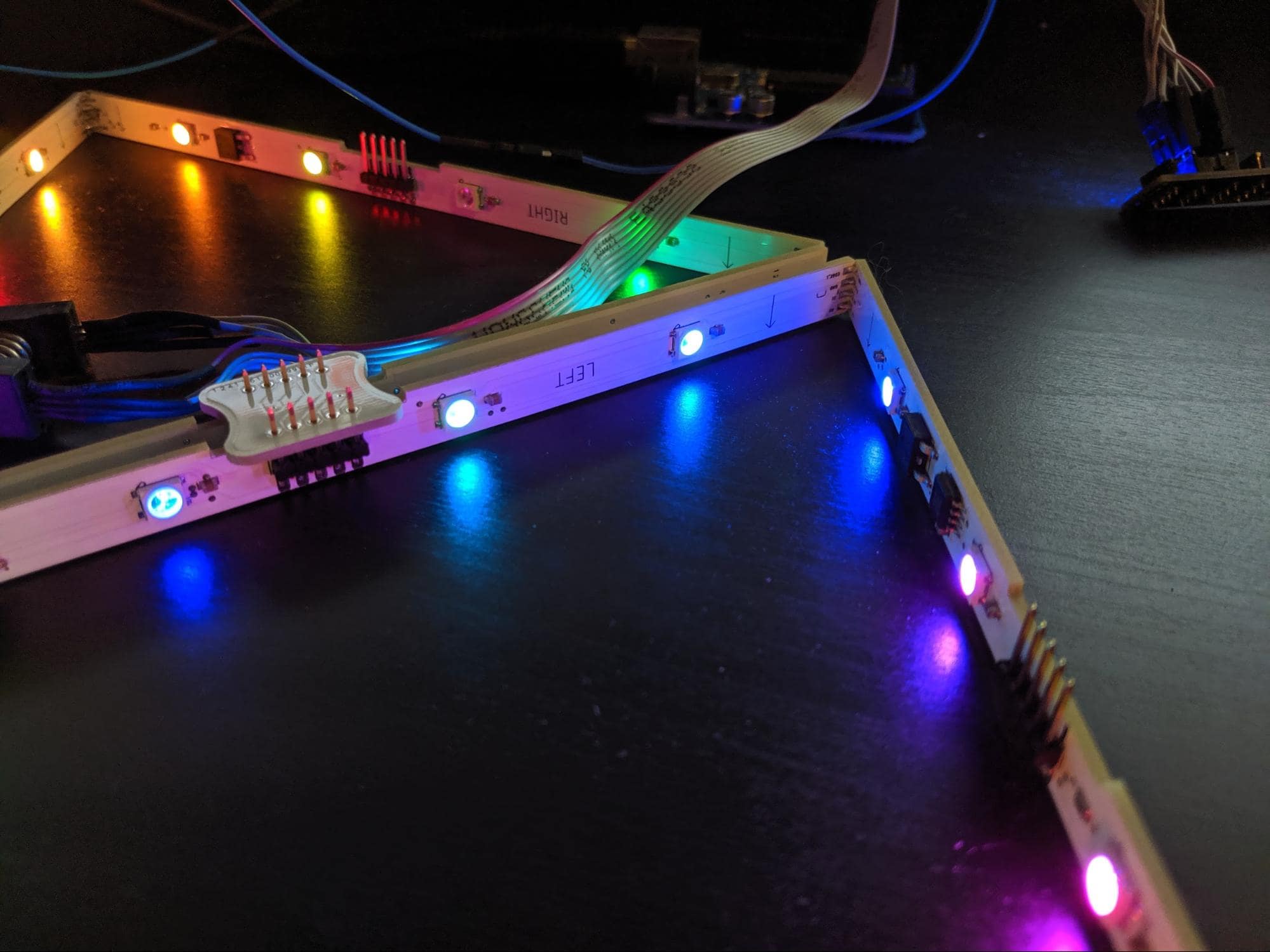
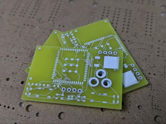
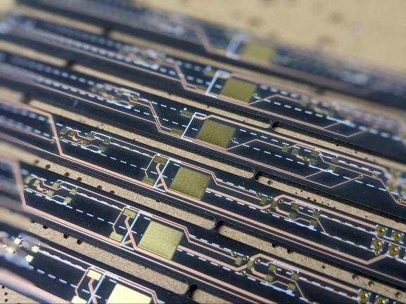
This photo shows several prototype PCBs assembled together
Using CNC Machining to Create Prototype PCBs
The first technology is one that is useful just for prototyping and it is a technology this article has covered already: CNC machining.
CNC machining can be used to mill traces and holes out of copper-plated blank boards to create prototype PCBs. The technology used for milling PCBs is basically the same as the one used to mill parts from wood, plastic, metal, et cetera.
However, the machines themselves are a bit different. PCB mills are designed to use the tiny end mills required to make intricate traces and small-diameter holes needed to make PCBs.
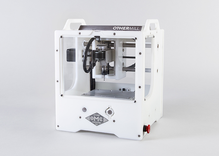
This is the Othermill by Bantam Tools. The Othermill is a CNC mill made specifically to make prototype PCBs
The video below, from Adafruit Industries, shows a PCB mill being used to create a two-layer prototype PCB.
The standout benefit to milling PCBs is speed. A prototype PCB can be made on a PCB mill within a few hours depending upon the size of the PCB. Even the fastest quick-turn PCB manufacturing services (we will get to that in a moment) take a couple days to have your prototype PCB shipped and delivered.
However, PCB milling does not offer nearly the same quality that traditionally-manufactured PCBs do. Only high-end PCB mills using extremely small end mills can replicate the trace width available from normal PCB manufacturing; otherwise, on most PCB mills, the boards will have larger traces. For the same reason, PCB mills cannot generally be used to make boards for fine-pitch SMD components.
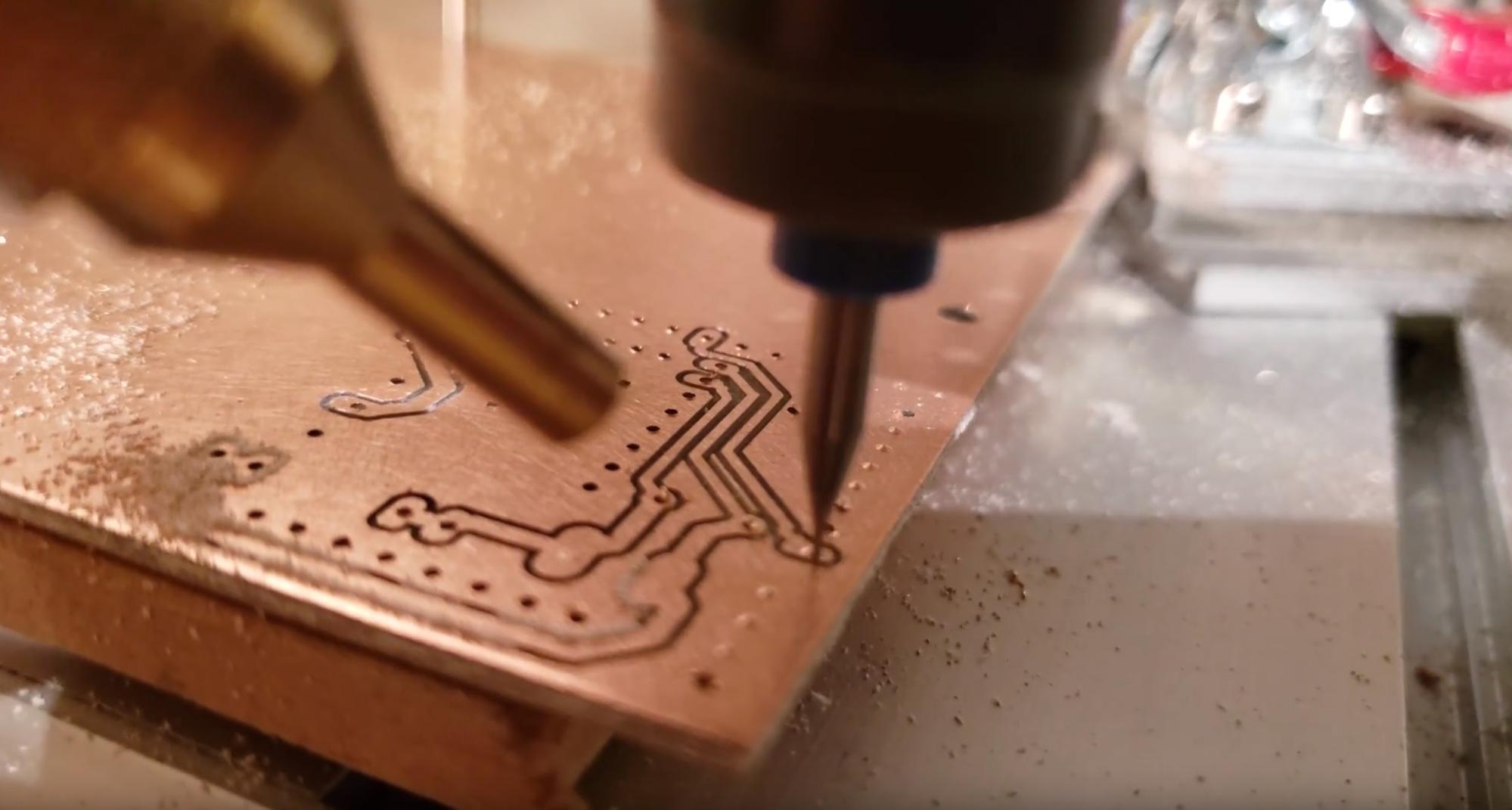
This is a prototype PCB being milled from a piece of copper-plated FR-4
Another downside to milling PCBs is that the PCBs lack a solder mask. Solder mask is a coating that is applied to most PCBs to cover all areas of the PCB other than contact points for attaching components. Solder mask is what gives many PCBs their green color. Solder mask prevents solder from sticking to parts of the board where solder is not meant to be applied. This means that milled PCBs can be more difficult to solder and solder bridges have a greater chance of forming and creating short circuits.
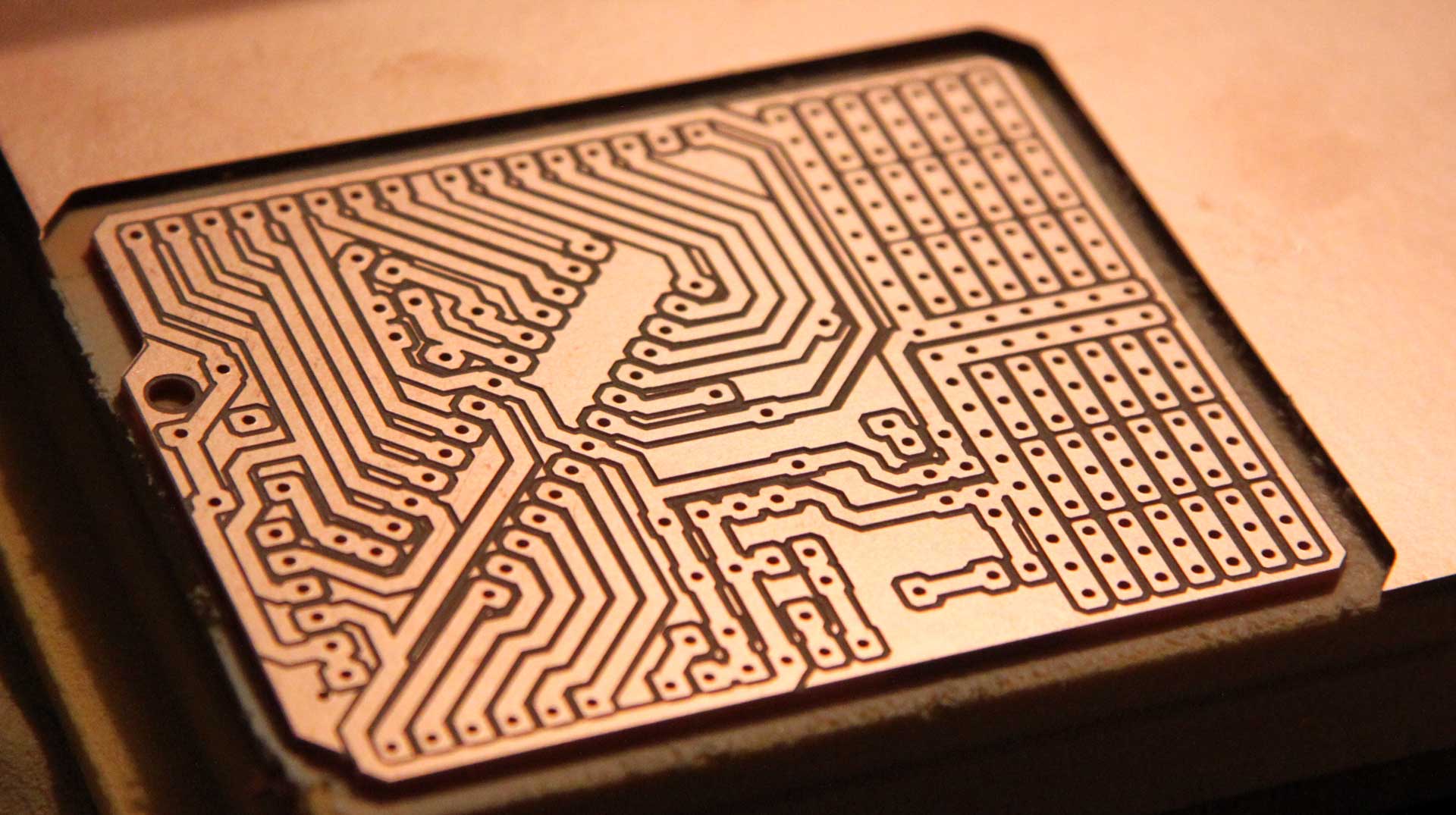
Milled PCBs lack solder mask, which can make soldering components more difficult and the chance of forming a solder bridge higher
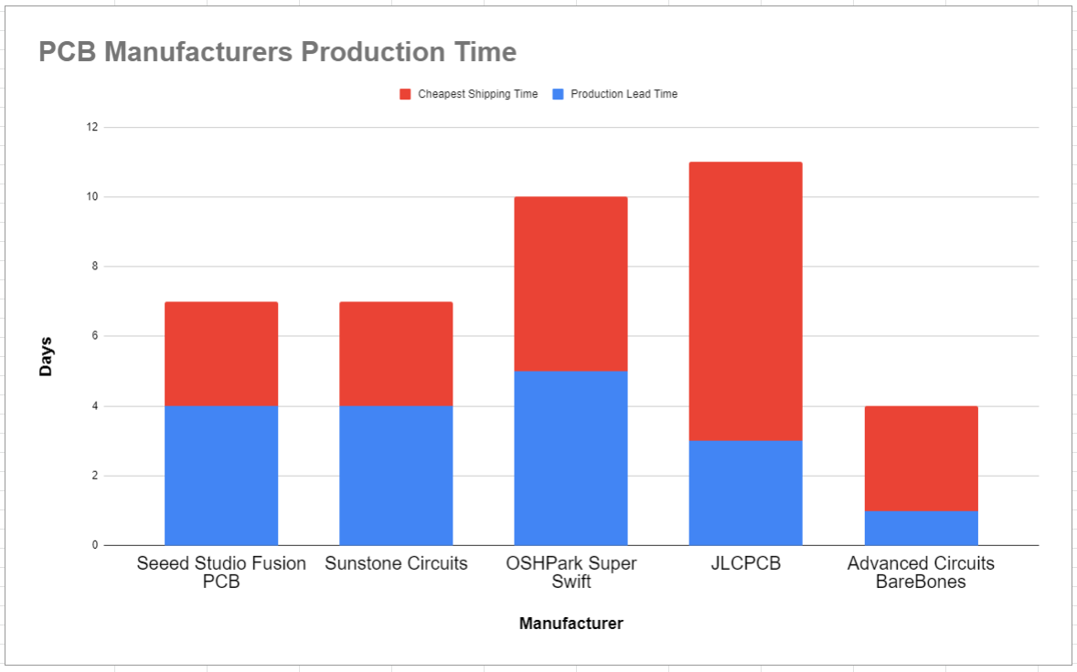
Prototype PCBs From Quick Turnaround Services
The next step up in PCB quality from CNC milled PCBs is a specific and unique quick-turn PCB manufacturing service called Bare Bones PCB by Advanced Circuits. The Bare Bones service uses a chemical etching process to produce PCBs, the process used for almost all PCB production.
However, in order to reduce the time required to make PCBs down to only one day, the Bare Bones PCB service does not apply solder mask, or a silkscreen. The service also does not support internal cutouts in PCBs. By cutting these steps out of the traditional PCB manufacturing process, the Bare Bones service is able to offer an extremely fast one day then around time.
The quick delivery time is the biggest benefit of using Advanced Circuits' Bare Bones PCB service. Having PCBs manufactured the traditional way usually takes a couple of weeks between the time your order is placed and the time your boards are delivered. Being able to get your PCBs more quickly means your product development cycle can also move more quickly, with less time between prototype iterations.
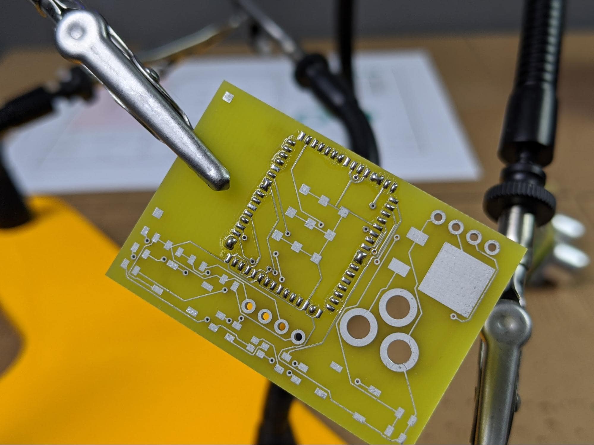
Compared with CNC milling PCBs, the Bare Bones PCB services offers the advantage of being able to produce smaller trace widths and footprints for fine pitch components. In the image above, you can see that the traces are much narrower than the ones in the CNC-milled PCBs.
However, both the CNC and the Bare Bones PCB prototyping technologies lack solder masks and, as mentioned previously, this means soldering is more difficult and more prone to electrical failures. Accidentally forming solder bridges is actually even easier to do with PCBs produced by the Bare Bones service than they are with milled boards because the Bare Bones service can utilize more closely-spaced traces.
Prototype PCBs from Full-scale Production Companies
Finally, prototype PCBs can be made using the same processes as PCBs at full-scale production, just at smaller quantities. There are a large number of PCB manufacturers from which to choose but they all make PCBs using roughly the same process. The process is complex and involves a range of different technologies. The video below, by Strange Parts on YouTube, is a tour of a PCB manufacturer in China.
As mentioned in the video, many PCB manufacturers take orders from multiple different customers and combine them into a single, large panel for manufacturing. This means that, for prototyping purposes, PCBs can be ordered from the very same companies that might also manufacture your product at scale one day.
This photo shows a set of prototype PCBs made from OSH Park
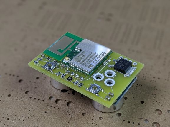
This is another prototype PCB example. This one was made by Seeed Studio Fusion PCB
The biggest benefit of having PCB prototypes made using processional manufacturing techniques is that their construction and performance will be the same as for production boards. For later prototyping stages, getting the final prototypes to be as close as possible to the final product is critical for avoiding unforeseen problems with a production part.
Using professional PCB manufacturing technologies ensures that your prototype PCB is as close as possible to the final design for your product.
The most significant downside to using PCB manufacturers for prototyping is the time it takes between placing an order and receiving your boards. This is especially true for batch PCB services, in which your order will be placed in a panel with potentially numerous different designs.
It might take a PCB manufacturer several days to put together a panel, another couple days to actually produce the parts and a few more days for shipping. This can all add up to a couple of weeks between each prototype version, slowing down the development of your product.