Learn all about Panelizing PCBs and up the manufacturing process of your next projects!
You've planned out your electronics on a breadboard, done all the research for part selection, designed a printed circuit board, verified all the airwires are routed. You are ready to get your PCB manufactured!
You may even have prior experience with getting boards made. Ordering single PCBs is not too difficult. Simply upload an Autodesk EAGLE BRD file or a set of Gerber files to your PCB manufacturer of choice, depending upon their requirements, and get finished, blank PCBs on your doorstep a little while later.
Assuming you’ve done all the work involved in designing a PCB, ordering single PCBs is not too difficult.
Ordering individual PCBs this way is perfectly fine for prototypes and small-scale projects, but as you move towards manufacturing at scale, it will become useful, and sometimes necessary, to add one additional step to your design process, panelizing your PCBs.
What is PCB Panelization?
PCB panelization is an important manufacturing technique where multiple PCBs are attached together and manufactured en masse. Sometimes, these PCBs are simply multiple copies of the same design, replicated over and over and produced together; this is the type of panelization we will be doing in this article.
A panel can also be created from multiple, different PCB designs. By panelizing a PCB, a group of PCBs can be made and assembled together. Placing the PCBs into the panel has several advantages for manufacturing the PCBs themselves and for populating the PCBs with components.
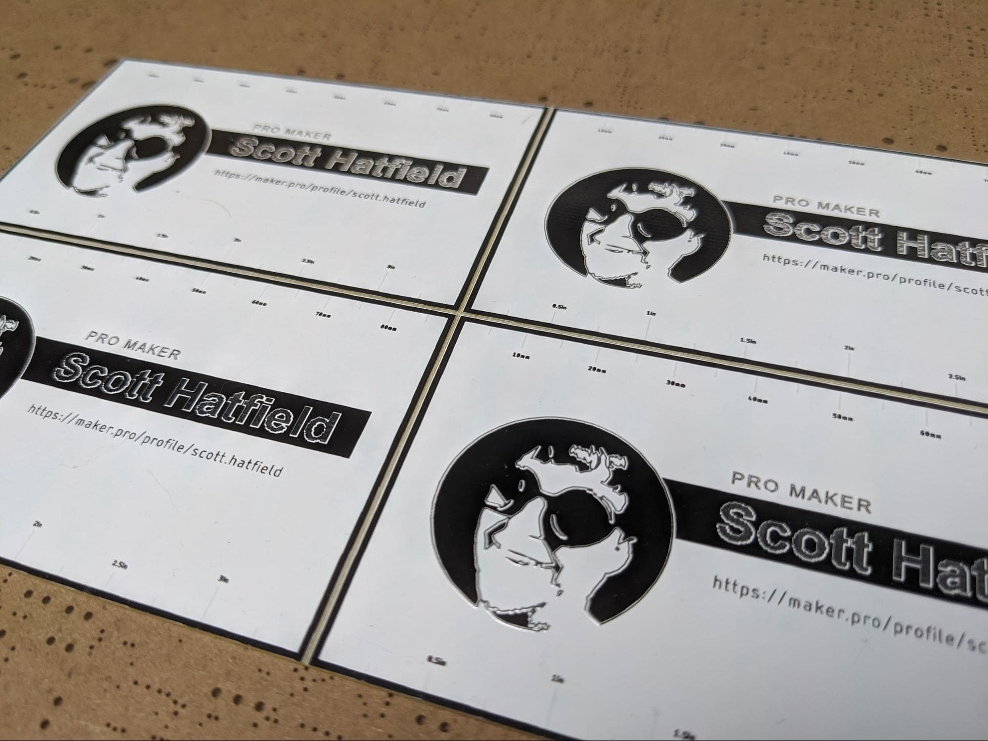
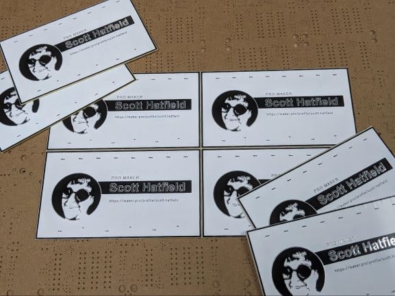
This photo shows a 2x2 panel of PCB business cards.
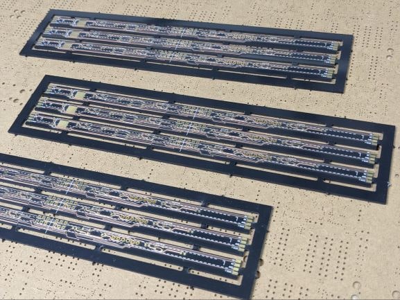
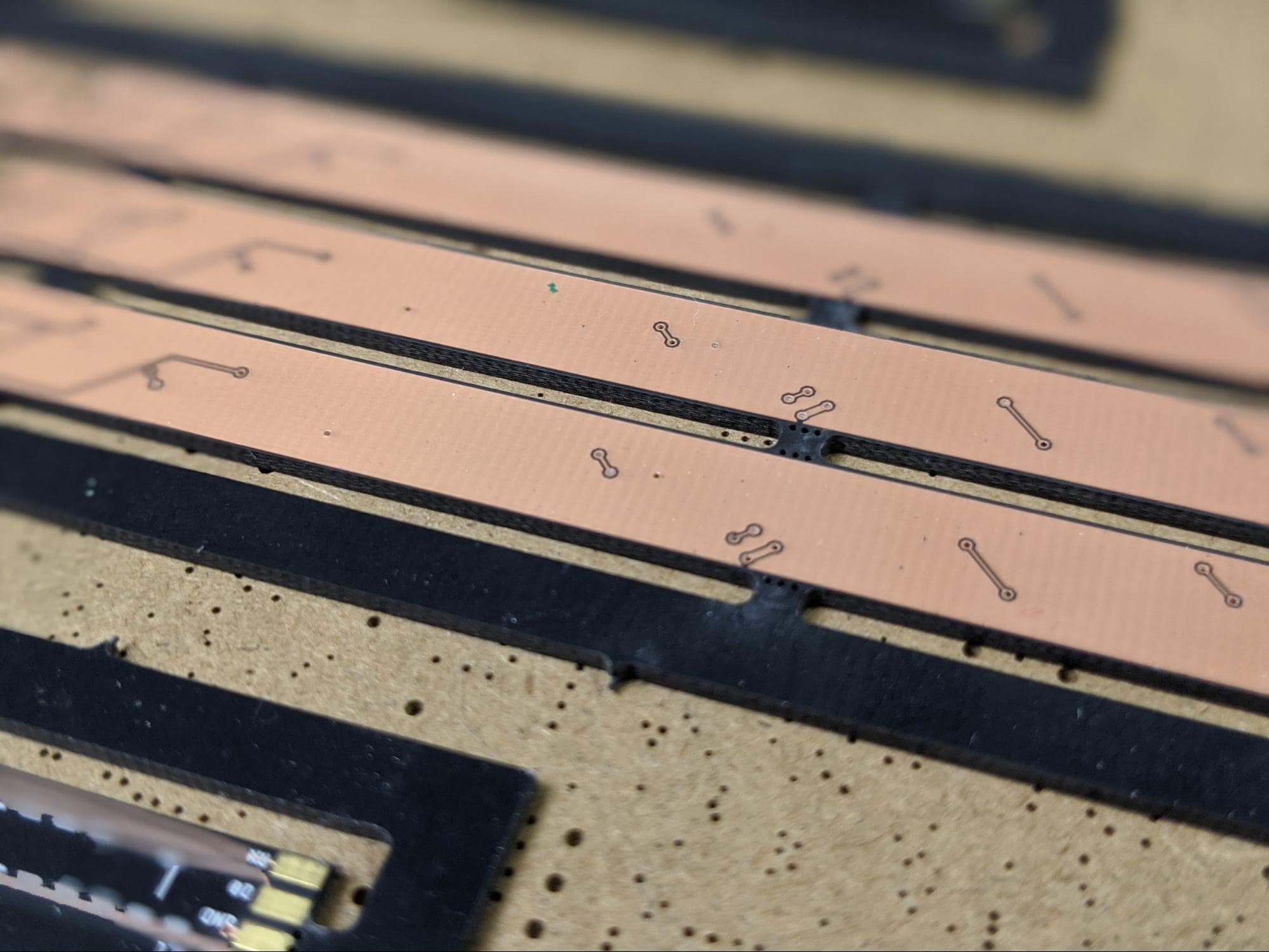
These PCB panels each have three copies of a PCB and a frame surrounding the entire panel
Advantages of PCB Panelization
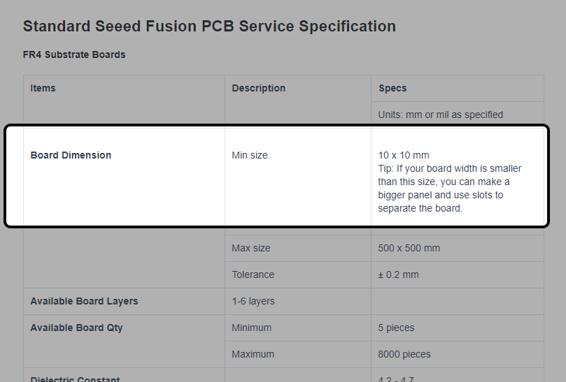
Panelization has a number of benefits compared with manufacturing PCBs individually. First of all, panelization is sometimes required to get a board made. Every PCB manufacturer will have specifications for the minimum board size they are able to produce. This limitation is typically directly related to the capabilities of the machinery the manufacturer uses.
So, if you are making a very small, or very thin, PCB design, you might have to create a panel in order to comply with the requirements for your manufacturer.
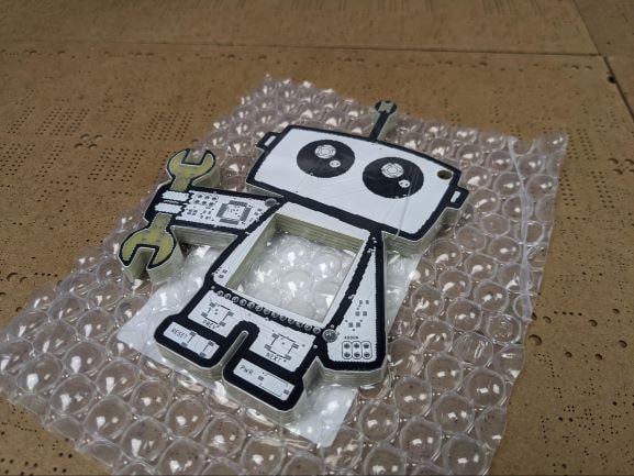
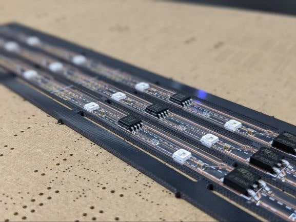
These PCBs are only a little wider than an ATtiny85, so they need to be placed into a panel in order to be manufactured. Otherwise, the individual PCBs are too narrow to be made.
A second advantage to panelization is that it makes manufacturing and assembling larger numbers of a PCB design more cost effective. This advantage comes into play as you prepare to have your electronics mass produced.
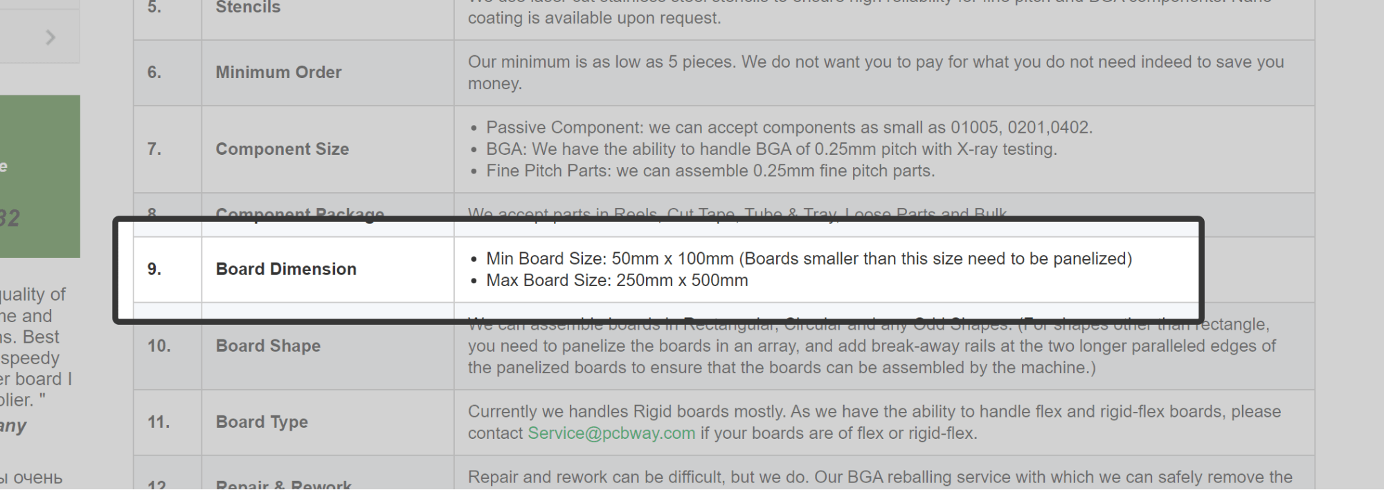
Panelization allows a greater number of boards to be assembled at once by pick-and-place machines which, again, can greatly reduce the per-unit cost of manufacturing. Often, PCBA services have a minimum board size for assembly that may be larger than your individual PCBs. For example, PCBWay requires boards larger than 50mm x 100mm for assembly. If your PCB is smaller than this, it will need to be panelized.
PCBWay requires boards at least 50mm x 100mm for assembly.
Panelization in Batch PCB Services
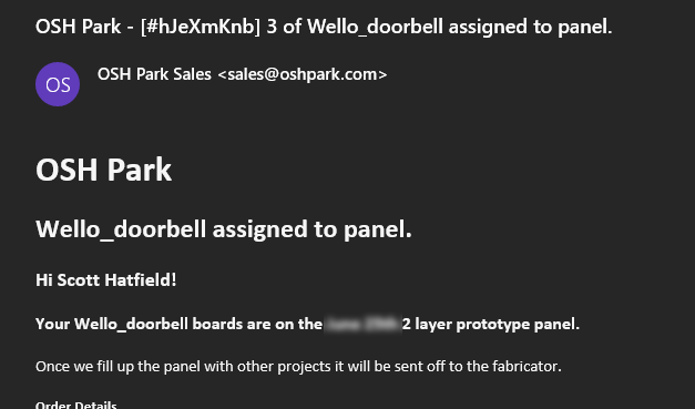
If you've ordered PCBs from services like OSH Park, for example, your PCBs were likely manufactured in a panel. If you take a look at boards made by OSH Park, you will notice little rough sections on the edges of the board, or even small tabs still attached to the boards. These are places where your PCB was connected to others in a panel.
These little leftover bits of FR4 are colloquially called mouse bites. They are often left over after removing individual PCBs from a tab route panel.
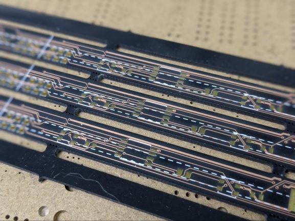
This photo, from OSH Park (@OSHPark) shows a full PCB panel made from many different PCB designs
When you place an order with OSH Park, your PCB is assembled with many others into a large panel before being sent to the manufacturer. OSH Park is quite transparent about this procedure. As part of the ordering process, you will receive an email when your board is placed in a panel.
Panelizing orders from multiple customers is a major part of the strategy OSH Park and similar fabs use to deliver affordable PCBs at prototype quantities.
PCB panelization is an electronics manufacturing technique in which multiple PCBs, whether they are all identical copies of the same design or multiple, different designs, are placed into a single sheet and manufactured all at once. Then, after the bare PCBs are made and populated with components, the boards can be snapped apart to separate them from the panel.
These PCB business cards were manufactured in a panel and then snapped apart to end up with individual boards.
Panelizing PCBs has a number of advantages compared with manufacturing and assembling boards individually. First, panelization is sometimes required to have a PCB made. This is especially the case if your PCB design is particularly small. The equipment used to manufacture and assemble PCBs is often unable to work with boards that are too small. By assembling several small boards into a panel, the total size of the panel can be made large enough to work with PCB manufacturing equipment.
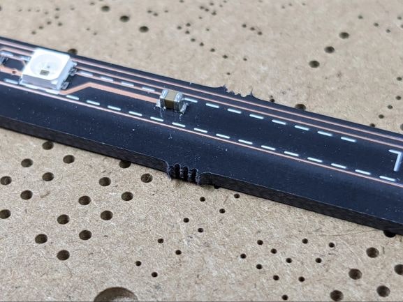
These PCBs are only 7mm thick, so they need to be placed into a panel to be manufactured.
Panelizing PCBs also reduces the per-board cost of assembly because multiple PCBs can be assembled at once. This economy of scale mainly applies to large volumes of PCB manufacturing.
There are two main PCB panelization methods that I will introduce in the next article in this series.