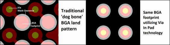
The use of Via-in-Pad technology for high-density BGAs
Via in pad guidelines
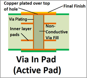
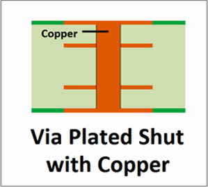
1. Plug the via by resin and plated it flat by copper.
It is suitable for small BGA via in pad. This process fills the via hole with a conductive or non-conductive material and then the via surface is plated over, providing a smooth flat for a solderable surface.
These are used for via-in-pad designs where a component can be mounted over the via, or a solder joint will extend over the via connection.
TIP: A common misconception is that a non-conductive fill will either not pass any or only a very weak electrical signal through the via.
This is not true. The barrels of the vias will still be plated with copper the same as any other via on the board, the only difference is the empty air in the barrel is replaced with the fill material.
This is usually done to prevent solder or other contaminants from entering the via or provide structural support for a copper pad covering the open hole in the case of a Via In Pad.
Process capability:
- Min Drilling: 0.20mm (Aspect Ratio = 8:1)
- Min Pad for VIA: Drill + 0.15mm
2. Microvias and via in pad plated over.
According to IPC, a microvia is a hole with a diameter of < 0.15mm. It can be a through via hole (with all respect to an aspect ratio), but we normally see them as blind vias between 2 layers. Mostly drilled by laser but some PCB manufacturers are also drilling microvia with a mechanical drill bit. It is slower, but the holes have a clean and nice cut.
The microvia copper fill process is an electrochemical deposition Process applied in the manufacturing of a multilayer process, also called capped vias. The process is complex. Copper filling of microvias is available from most PCB manufacturers that are capable of producing HDI PCB Boards.
Process capability:
- Laser Drilling: 0.10-0.15 mm (Aspect Ratio = 1:0.8)
- Mechanical Drilling : 0.15-0.2 mm (Aspect Ratio = 8:1)
- Min Pad for VIA: Drill + 0.15mm