Almost in any circuit design, building at least one regulation stage is necessary
Almost in any circuit design, building at least one regulation stage is necessary. Two power supply design options are available, which are linear and switching. The linear regulators are easy to build but inefficient, especially when there is a high difference between the input voltage and the desired output voltage. Also, by increasing the regulator output current, the efficiency also decreases. Both of these problems are easily visible in terms of heat dissipation.
The switching regulators are very efficient but improper design and filtering could inject some amount of noise to the regulator’s output.
There are many switching design options, but the TI company introduced a good chip which I will discuss it in this article. According to the datasheet: “The TPS54331 device is a 28-V, 3-A nonsynchronous buck converter that integrates a low RDS(on) high-side MOSFET. To increase efficiency at light loads, a pulse skipping Eco-mode feature is automatically activated. Furthermore, the 1-μA shutdown supply-current allows the device to be used in battery-powered applications. Current mode control with internal slope compensation simplifies the external compensation calculations and reduces component count while allowing the use of ceramic output capacitors.”
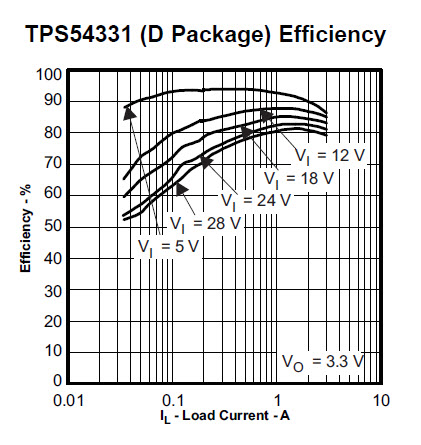
The output voltage of the regulator even could be as low as 0.8V. Also, it introduces a high switching frequency (570KHz), which is good. The figure-1 shows the efficiency chart in relation to the output current and input voltage.
Figure-1,
Efficiency chart, the output voltage has fixed at 3.3V
The chart clearly shows that the highest efficiency (near 95%) satisfies when the input voltage is around 5V (the output has fixed at 3.3V) and the output current somewhere between 100mA and 1A. in most digital circuits, the input voltage is 12V, therefore the efficiency parameter would be something around 88% (1A current).
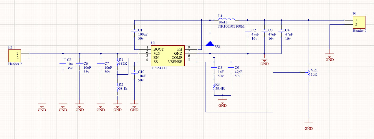
The datasheet of the TPS54331 provided a table which defines the output voltage by modifying two resistor values, but in this article, I made the output variable. So you can adjust the output by turning a multiturn potentiometer. Figure 2 shows the schematic diagram. By turning the VR1 potentiometer, the output voltage would change.
Figure-2,
Schematic diagram of the switching voltage converter
The schematic has drawn by the Altium designer, but you are not bounded to use this software. Just look at the schematic and re-design it in your own favorite CAD software.
Be careful to select suitable voltages for the input and output capacitors. In the schematic, I defined the input to be 12V, and therefore the output would not exceed 12V. try to select high-quality XR5 capacitors for the output (C2, C3, and C4). Try to keep the component pins short, preferably use the SMD component and place them as much as close to the chip. Use two layers PCB and allocate one layer completely for the ground.
If you desire that your design complies with the EMC rules, please make sure that you connect the ground of the regulator circuit and your main circuit at only one point. The switching currents of the switching power supply should not share a common ground with the rest of the circuit.
If you use a single PCB for all parts of the circuit, keep the power unit far from the sensitive blocks such as analog circuits.


