Maker Pro
Maker Pro

Wireless power transmission

Hi,

I am attempting to develop a system that will transmit wireless energy through use of 2 tuned inductors. I have below what is apparently a 'simple' circuit and was hopping for someone to shed some light on its operation.

I will tell you what i think is happening and perhaps someone can rip apart my theory.

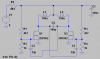
I assume the voltage applied is DC and we want to convert it to AC using what looks like a push pull power oscillator. so the current goes down all 3 of the connections. hitting the potential dividers it puts a foward voltage accross the gate and source of the N type mosfets which allows current to flow from drain to source. At the same time it charges the capacitor which prevents any more DC current from flowing. The right hand mosfet has more voltage at its gate and so more current can flow when the mosfet switches on.

okay so the inductors again split the current as the inductors see the sudden increase in current they resist it, a back emf is produced which slows down the current until the current change stops and so the EMF prodced is zero. The current is then constant and so the inductor simply acts like a short circuit. I can't work out what happens next? The inductor then must discharge creating a emf in the opposite way and a decrease in current which would give us a sort of AC wave or at least a varying current wave. what causes it to discharge?

I assume c4 is a tuning capacitor..... and that the mosfets switch on and off somehow surely they must switch on and off at different times too? what causes this? , where would i connect the load? in parallel with c4 perhaps??

any help much appreciated. I suppose alot of things that i have said is utter rubish so be nice.

Thanks,

Lee.
 

Attachments

  • Circuit.png
    Circuit.png
    24.9 KB · Views: 1,871

CDRIVE

Hauling 10' pipe on a Trek Shift3
I should tell you from the get go that wireless power transmission is possibly the most power hungry, power wasteful concept that was ever conceived.

Chris
 
I agree with Chris.

Also this already exists.

Though the convenience would be nice, it's not that hard to plug something in, and the power consumption is going to be 5-10 times (low side if you ask me) what you actually need to charge the device. The "wireless" chargers they sell these days are mostly cases that have metal points of contact for the pad that charges them or they use an inductor system like you have listed,but they are power hungry, and have caused device failure due to strong fields (specifically iPod classics which still use spinning disc hard drives)
 
Thanks for the replies.

I know that this type of power transfer is inpractical and probably useless but i want to do it in anyways, god loves a trier. I will move on to microwave transmission eventually but i have to start somewhere. I also know about the advancements intel have made and will be studying their reports in the weeks to come. For now i need to know how the circuit works or if someone can direct me to an inverter circuit that produces a half decent sinewave and perhaps give an explanation, that would be great.
 

CDRIVE

Hauling 10' pipe on a Trek Shift3
Yes, the operative terms in that article are "large coils" and they do mean large and tubular, like antenna elements. That said, the 80% efficiency is a hell of a lot greater than when I first read about this technology. I still don't consider 80% good at a time when we're trying to make efficiency a primary goal.

Chris
 
Where did you get the circuit from?

The two inductors L1 and L2 should idealy be wound with bifilar wire so they have very tight coupling between the two halves of the coil

The circuit works as an oscillator tuned by C4 and with C2 and C3 providing the feedback.
R5 will limit the output.
 
Yes, the operative terms in that article are "large coils" and they do mean large and tubular, like antenna elements. That said, the 80% efficiency is a hell of a lot greater than when I first read about this technology. I still don't consider 80% good at a time when we're trying to make efficiency a primary goal.

Chris
Well, 80% is in the same league as a typical wall-wart, perhaps even better, and that was at 1m, the efficiency is higher for closer distances. Intel is actually pushing for this technology commercially. I think it will take the form of a mat with the coil inside that you can just throw your cell phone or lap top on top of and it will charge.

Bob
 
Where did you get the circuit from?

The two inductors L1 and L2 should idealy be wound with bifilar wire so they have very tight coupling between the two halves of the coil

The circuit works as an oscillator tuned by C4 and with C2 and C3 providing the feedback.
R5 will limit the output.

thanks for answering the question! could you perhaps give me a general step to step of what the current is doing and how it is working as an oscillator? what causes the mosfets to switch one after the other?? what do eople mean by feedback capacitor? I am a complete noob so any help at all is appreciated.

Thanks,

Lee.
 
You have not said where you got the circuit from, did you read what I posted?

The two coils you show should be closely coupled together with the centre connction to the power supply. There may be enough interwinding capacitance to eliminate the tuning capacitor.

An oscillator is an amplifier with some of the output fed back to drive the input. You will see that there is a capacitor from each drain to the opposite gate. These provide the feedback.
When the device is first switched on, a small biasing voltage is fed to the gates to make the fets pass some current. One fet will pass a little more current than the other so the drain source will be a little lower than the other, this means that the other collector will rise and the first fet will be turned hard on by the feedback capacitor.

At some stage the fet will run out of breath and the tuned circuit will switch the other way so a continuous oscillation occurs.

Fets are very efficient switches and may not limit at a reasonable current. I presume that the resistor in the power supply is there to provide some current limit at the expense of power loss.
 

CDRIVE

Hauling 10' pipe on a Trek Shift3
I would expect efficiency for most common iron core transformers to be >=95%. I know that grid transformers are near 98%.

Chris
 
You have not said where you got the circuit from, did you read what I posted?

The two coils you show should be closely coupled together with the centre connction to the power supply. There may be enough interwinding capacitance to eliminate the tuning capacitor.

An oscillator is an amplifier with some of the output fed back to drive the input. You will see that there is a capacitor from each drain to the opposite gate. These provide the feedback.
When the device is first switched on, a small biasing voltage is fed to the gates to make the fets pass some current. One fet will pass a little more current than the other so the drain source will be a little lower than the other, this means that the other collector will rise and the first fet will be turned hard on by the feedback capacitor.

At some stage the fet will run out of breath and the tuned circuit will switch the other way so a continuous oscillation occurs.

Fets are very efficient switches and may not limit at a reasonable current. I presume that the resistor in the power supply is there to provide some current limit at the expense of power loss.

Circuit video

circuit schematic / article

http://www.vk2zay.net/article/253
and
http://www.vk2zay.net/article/262

I always just assumed the 2 coils were a centre tapped primary coil so the coupling would be pretty good?????

I understand up to the point that the right hand fet (U2) is allowing more current through because the voltage at its gate is bigger due to R3 being smaller than R1. I also assume that because the drain source voltage is bigger on U2 there is a positive potential on the right hand side of C4. As the gate voltage is also bigger on U2, C3 should charge the fastest??? when this is fully charged does it stop current flow somewhere is this the feedback you speak of?

"this means that the other collector will rise and the first fet will be turned hard on by the feedback capacitor"

I can see that the capacitors are connected from the gate of one Mosfet to the drain of the opposite but how does this provide feedback surely C2 and C3 both charge when the circuit is turned on ??

why does the FET 'run out of breath' because one of the capacitors has discharged? if current is continous does it not just charge as soon as it has discharged?

although i am not worrying about the purpose of r5 you have made me curious. 'They may not limit at a reasonable current' are you saying we are restricting the gate current so that the current from drain to source is not massive?

thanks again
 
C2 and C3 will both charge when switched on but they will not be identical and the fets will also differ. The fet that passes the most current will pull its drain voltage down which will lift the voltage at the other end of the inductor. This will pull the gate voltage more positive on the enthusiastic fet so it will be turned hard on.

The feedback capacitors cannot charge continuously since there is a limited voltage. When the voltage stops rising, it will be pulled low by the bias resistors and the circuit will switch over rapidly.

The frequency of operation may be determined by the feedback capacitors or the limit of the drain current due to the fet resistance.

You still have not said where you got the circuit.
 

CDRIVE

Hauling 10' pipe on a Trek Shift3
C2 and C3 will both charge when switched on but they will not be identical and the fets will also differ.

This is an issue that should be mentioned when simulating a flip flop like this. Unlike in the real world components in spice simulators can be identical. That's why the simulations sometimes fail to oscillate. When siming it's a good idea to intentionally unbalance the circuit.

By the way, I looked through those links that Ledwardz posted. I want to know how that guy broke into my shop? That looks exactly like the surface of my work bench! Utter chaos!!!

Chris

Thanks for this, when simulating i will put charge on the capacitor before i press play! It also appears that all engineers have messy work benches........
 

CDRIVE

Hauling 10' pipe on a Trek Shift3
Thanks for this, when simulating i will put charge on the capacitor before i press play! It also appears that all engineers have messy work benches........

The ones that don't aren't usually doing anything.

Chris
 
C2 and C3 will both charge when switched on but they will not be identical and the fets will also differ. The fet that passes the most current will pull its drain voltage down which will lift the voltage at the other end of the inductor. This will pull the gate voltage more positive on the enthusiastic fet so it will be turned hard on.

The feedback capacitors cannot charge continuously since there is a limited voltage. When the voltage stops rising, it will be pulled low by the bias resistors and the circuit will switch over rapidly.

The frequency of operation may be determined by the feedback capacitors or the limit of the drain current due to the fet resistance.

You still have not said where you got the circuit.

This still isn't sinking in. i agree with the first sentence. The fet that pulls the most current will pull its drain voltage down? the 2 inductors are in parallel how can it be pulling a different amount of voltage as its DC. The potential will always be a certain value above U2 which will be the same potential above U1??

Needless to say i don't get how this pulls the voltage at the other side of the inductor high. Is this between the inductors or above U1? then the gate voltage is higher on mosfet U1?

the capacitor bit again, i agree with the first sentence the capacitor should only charge up to the same voltage of that across R2 or R3 depeding on which capacitor you are looking at. pull down?

damn this is begginning to annoy me. Is there somewhere simpler i can start with perhaps a hartley oscillator and build up from there. I basically just want an AC signal from a DC signal without using PWM how hard can it be? I thought this would be a doddle with circuits everywhere. clearly not.

Cheers again
 
Sorry about not reading your post properly, I saw youtube and passed the references by as I have narrow band, not broadband!

The two inductors are in series and should be coupled closely together. The centre is at a constant potential, so when the voltage on one side goes down, the voltage at the other end goes up. Think of a see saw.

You will not find a much simpler circuit than this.

To start the simulation, you could make one bias resistor slightly different to the other. This will not be necessary in practice since there will be natural differences.
 
Hmm - maybe if you started with a conventional wired power source, then shortened the distance to the receiving end, you would need less wire - get it? - wire less / less wire ...

... ok I'll go back to my corner now.....
 
Top