Maker Pro
Maker Pro

Why put MOSFET's on negative side vs positive of motor

I was just curious, most things I see about how to set up a mosfet say to do it something like this:
mosfet.gif


So typically it's the negative side of a motor goes to the MOSFET drain side. It's basically acting like a switch. So why switch the negative vs the positive side of the motor?
 

Harald Kapp

Moderator
Moderator
Your image doesn't show...

The voltage that controls the MOSFET is applied between gate and source. If you put the load into the source path, the Gate voltage needs to be higher because it has to include the voltage drop across the load, compare the circuits in this schematic:
blabla-png.13584

Vgs2 is a few volts for a typical MOSFET. Assuming Vds ~0v for a M2 being fully on (Vgs2>Vt where Vtthreshold voltage of the MOSFET), the load R2 sees Vbat and losses are small.
The circuit with M1 on the other hand would require Vgs1 to be as high or higher than Vbat+Vt to fully turn on M1. This requires a separate power supply for the driving circuit. Or, if you do not have a separate supply, Vgs1 can be only as high as Vbat, therefore allowing for V(R1) being only Vbat-Vt, considerably less than with the circuit around M2. This in turn means that Vds(M1) is much higher tan ~0V and M1 will dissipate lots of power.

I hope that clears matters.
 

Attachments

  • blabla.png
    blabla.png
    6.1 KB · Views: 1,220
Also to be noted that the left circuit is sometime preferred because he is more fail save. If a short to the GND happen the load is not supplied unlike with the right one.
 

KrisBlueNZ

Sadly passed away in 2015
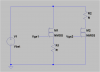
Here's the image from post #1. It doesn't show up in the thread here, but it came through in the notification email that I received for the thread.

mosfet.gif
So typically it's the negative side of a motor goes to the MOSFET drain side. It's basically acting like a switch. So why switch the negative vs the positive side of the motor?
The simple answer is that the MOSFET responds to the voltage between its gate and its source. Connecting the source to the 0V rail means that the input signal just needs to alternate between 0V and some positive voltage, typically around +12V. Such a signal is easy to generate, because all of the other circuitry will normally use the 0V rail as its negative supply.

The most that's needed is a level shifter to shift a logic-level signal (e.g. 0V/+5V or 0V/+3.3V) to a higher voltage (0V/+12V). If the MOSFET has the "logic-level input" or "low Vgs" feature, and saturates strongly enough with only 5V between gate and souce (or even less for some modern devices), a voltage shifter may not even be needed!

The same arrangement is used with P-channel MOSFETs - the source is typically connected to a positive supply rail, and the gate is driven with a signal that alternates between that positive voltage rail and a voltage around 12V lower. If the positive supply voltage is around +12V then the gate can be driven by a signal that alternates between 0V and +12V, which is easy to generate, and likewise, a logic-level input device may have its source connected to an even lower positive supply voltage.

This configuration is called "common source" and corresponds to the "common emitter" configuration for bipolar transistors. You can connect a MOSFET in common drain configuration (aka source follower) (equivalent to common collector, aka emitter follower, in transistor circuits) but this requires a higher voltage supply to provide the gate signal. Typically a charge pump or switching supply is used to create a rail around 10V higher than the positive rail that the MOSFET's drain is connected to.

This is because saturating a MOSFET requires a significant amount of voltage between gate and source, whereas a transistor that's conducting a heavy current typically has less than 1V between base and emitter. The output of an emitter follower could be as much as 1V less than the input; this voltage loss is often not a problem. But in a source follower, the gate-source voltage is a lot higher, and MOSFETs are normally operated in full saturation to gain the maximum benefit from their very low ON-resistance (RDSon) and this requires the extra positive voltage rail. Conversely, transistors in the emitter follower (common collector) configuration are not normally saturated, and the small base-emitter voltage drop is tolerable.
 

(*steve*)

¡sǝpodᴉʇuɐ ǝɥʇ ɹɐǝɥd
Moderator
Incidentally, there is no reason why you can't use an N channel mosfet to switch the positive lead of a load (a motor in this case) if you can arrange to have a power supply that can go sufficiently positive with respect to the source of the mosfet.

This may be achieved by having the power supply to the logic with its ground rail tied to the source of the mosfet (and therefore floating with respect to the power supply for the load) or by creating another power supply which is controlled by some level switching circuitry. Some mosfet gate drivers allow this by providing their own source for gate voltage by means of a switched capacitor inverter or similar. This rail will be above the +ve voltage or -- less frequently -- below the ground rail for the load.

The real issue, as Kris points out, is whether you can get an appropriate voltage swing to the gate.
 
The benefit of using a N-channel versus a P-channel in either configuration low side or high side, is N-channel devices generally have a lower Rds(on). So for high power circuits the N-channel is preferred. But high side switching can increase the complexity of the design.
Adam
 

(*steve*)

¡sǝpodᴉʇuɐ ǝɥʇ ɹɐǝɥd
Moderator
For more detail, here is a device that allows you to use N channel mosfets as high side drivers.

Even if you don't understand the details, you'll note the added complexity which designers try to avoid unless it is required.

Arouse1973 --> *snap*
 
You can use a P channel mosfet to switch the positive supply but the input is reversed, 0V gives no current for n channel but full current for p channel.

Also, your positive line can be up to 60V which is more than what the base/ source of the P channel can stand so extra components would be needed to limit the voltage.

Yes indeed gate / source is only +/-20V in this case so you have to be careful.
Adam
 
ok, makes sense. Thanks for clarifying. It just required I understand the inner workings of a mosfet a little better. :)
 
Added to which P-channel mosfets are generally more expensive than equivalent N-channel mosfets. Add the additional circuitry required and they become unattractive cost-wise.
 
Top