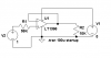
Having a look at the data sheet the capacitance graph only goes to 10nF and needs a resistor over 100R. I would get rid of it.
Well, butter my buns! You're right! Figure 4-4 in the data sheet.
I'm very surprised. The closed loop output impedance of the op-amp should be very low - under an ohm, I would expect. I would have thought that 47 ohms to a capacitor was by comparison a very weakly coupled load, and the op-amp would be able to handle it easily.
I've done some research, and discovered that the op-amp's ability to drive a capacitive load is proportional to the closed loop gain. So a buffer is the worst case. I also noticed that the typical op-amp output impedances used in the examples are much higher than I thought they would be - 50 ohms in one case, and that's for a buffer. I don't see how the output impedance of an op-amp buffer stage can be so high... Can you explain, Adam?
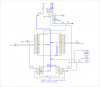
But I have just noticed an even bigger problem which might explain the strange behaviour of the op-amp.
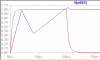
The OP wasn't clear about where the problem is occurring. Like you, I assumed that he meant that there was a nonlinearity in the hardware, but I think the problem is in the firmware that reads the ADC and generates a corresponding PWM signal. So I don't think the op-amp is actually behaving strangely. But not sure.
The common op-amp buffer circuit that everyone uses, short out to non inverting input works ok for lowish impedance inputs that are varying d.c. This guy has got load of resistance on the non inverting terminal. this will cause issue if the feedback resistance is less than 100R. This upsets the input bias current and can cause the input protection diodes to short out the output causing the current limit circuit to cut in.
I'm pretty sure you have this backwards. The problem with the protection diodes conducting occurs when the signal feeding the non-inverting input has a low impedance and changes more quickly than the op-amp's output can slew. The feedback on the inverting input can't follow the non-inverting input, and a voltage difference appears between the inputs. For op-amps that have protection diodes (this one doesn't), you can prevent damage by putting a resistor in series with either input (or both), although this obviously can degrade frequency response.
So what you need to do is match the feedback resistor with the input resistance, but too high and you have issues with input offset currents.
Yes, input bias current is another reason why a resistor is sometimes connected in the feedback loop in a buffer circuit. The resistor is chosen to match the input signal's impedance, on the assumption that the input bias currents of the two inputs will be roughly equal and will produce roughly equal voltage drops across the two resistances (the source resistance and the feedback resistor), which will cancel out. This particular op-amp is a CMOS one, with bias currents measured in picoamps, so I don't think you need to worry about that! I would be more worried about the input offset voltage (4.5 mV max at room temperature).
Another problem is formed by this fix is the RC of the feedback resistor and input capacitance which causes ringing on the output. The fix for this is a small capacitor across the feedback resistor.
I don't see how the input capacitance can interact with the feedback resistance. They are connected to different inputs...
The standard op-amp buffer is ok with very slow changes in input voltage and as a d.c buffer. But with anything that's varying you have to be careful.
I don't think so! Buffer stages are often used with very high frequencies. Video, for example. But I take the point that they can be less stable than stages with higher gain, especially into capacitive loads.