Maker Pro
Maker Pro

Simple Circuit using transistors

One step signal 0v to 3.3v
Output Single pule signal 3.3v to 0v to 3.3v

Requirements:

1. Pulse width is in milliseconds range
2. simple and low cost
3. Find a solution that does not use logic gates, but only transistors
4. draw the time graph of all the nodes in the circuit that are switching.

I am having trouble with #1 and #4. I was thinking of using a mono stable multivibrator.
 

KrisBlueNZ

Sadly passed away in 2015
A simple way to convert a step input change into a pulse is with a capacitor-resistor "differentiator" or pulse generator. Feed the input signal through a capacitor, with a resistor to 0V. To calculate the values, choose a convenient resistance, say 10k, and calculate C by rearranging the formula t = RC where t is around 1 ms.

What is the shape and polarity of the signal at the output of that circuit, in response to the input changing from 0V to +3.3V?

How does this relate to the signal you need to produce at the output? Is the polarity the same, or is it inverted? Do you need to change the waveshape to give clean edges at the output?

How can you use one or more transistors to modify the signal from the C-R circuit to produce the specified output signal?
 
Thank you for the response,

The shape and polarity of the signal at the output in response to the input changing from 0v to 3.3v is:high low high

The signal at the output is inverted and I don't need to change the wave shape.

I am not sure about the amount of transistors, my first thought was a multivibrator circuit with a RC for the pulse output.
 

KrisBlueNZ

Sadly passed away in 2015
OK. Start with a C-R "differentiator":

c-r differentiator.gif

(That image is from http://www.electronics-tutorials.ws/rc/rc_3.html)

See what happens at the output in response to the input going from low to high? There is a positive pulse whose length is determined by the values of R and C.

How can you use one or more transistors to convert this positive pulse, with a clean rising edge but a slow falling edge, into a signal that's normally high (+3.3V), goes low during the positive pulse, then returns high again?

Does this circuit need to invert the pulse or not?

What transistor configuration(s) (common emitter, common base, common collector) might be able to do this conversion?

How would you set up the biasing so the circuit's output will be normally high, but will go low when the output from the C-R differentiator is positive?
 
upload_2014-5-25_8-20-26.png
Here's how the signals should look, a common emitter would give me the output signal, with a edge detection circuit? this would give me high then low output from the C-R.
 

KrisBlueNZ

Sadly passed away in 2015
Yes that's right. Can you draw up a circuit?

Remember that the base-emitter junction of the transistor will clamp its voltage to about 0.7V. If you connect the output of the C-R circuit straight to it, this clamping behaviour will affect the C-R circuit. What would you put between them so the C-R circuit won't be clamped, but the pulse will still cause some current to flow into the base of the transistor?
 

(*steve*)

¡sǝpodᴉʇuɐ ǝɥʇ ɹɐǝɥd
Moderator
That circuit will put both transistors in grave peril and give you an output that is always at 3.3V.

Contemplate load resistors and what currently happens when you put 3.3V on the base of Q1.

edit2: undo edit -- I misread one of the resistor values.
 

KrisBlueNZ

Sadly passed away in 2015
OK, there are quite a few problems with that circuit.

1. You have connected a voltage source directly across the base-emitter junction of the first transistor. A base-emitter junction behaves like a diode. Look at the current vs. voltage curve of a diode:
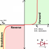
diode i-v curve.png

(That diagram comes from https://learn.sparkfun.com/tutorials/diodes/real-diode-characteristics)

See that in the top right quadrant of the graph, the diode current starts increasing rapidly when the forward voltage exceeds VF, which is about 0.7V for a silicon device. So if you connect a voltage of 3.3V across a diode (or base-emitter junction) in the forward direction, a very high current will flow. This would damage the transistor.

The simple way to prevent this problem is to add a series resistor, as shown here:

diode driven through series resistor.gif

(That diagram comes from http://electronicdesign.com/power/graphical-numerical-techniques-size-led-array-s-drive which discusses driving LEDs but the principle is the same for diodes)

The resistor, RX, will have 3.3V on the left end, and around 0.7V on the right end, so there will be about 2.6V across it. Ohm's Law can be used to calculate a suitable value for RX if you know how much current you want to flow.

Let's say we want 5 mA to flow into the transistor's base. Can you calculate an appropriate resistance for RX?


2. You don't actually need the first transistor. But that lesson is an important one, and will actually apply to the second transistor, so don't ignore it.

3. The time constant of a C-R circuit with 10 µF and 10k is 100 ms. The question calls for a pulse width in the "milliseconds range". I take that to mean something like 5 ms. Can you change the value of C to get a time constant of 5 ms?

4. The second transistor is connected directly between VCC and 0V. This is a problem if it ever gets biased ON. Also, your output is taken directly between VCC and 0V, which means it will always be 3.3V and will be unaffected by the transistors.

Have a look at the three configurations for a transistor amplifier.

Transistor configuration.JPG
(That image is from http://pdjinc.com/electronics_notes.html)

In each configuration, the transistor is connected across a supply voltage, but a resistor is also present. A resistor is normally needed when the output of the circuit needs to be a varying voltage.

A transistor is described as a current amplifier. In a common emitter circuit, the middle diagram above, current feeding into the base-emitter junction is amplified by the transistor and causes a higher current to flow in the collector-emitter path. In that diagram, R2 is used to convert the transistor current into a voltage.

One arrangement of Ohm's Law says that V = I R. So if R is constant (e.g. 10k in the diagram), this formula means that V is proportional to I. In other words, as the current through the resistor varies (due to the action of the transistor), the voltage across the resistor will vary in proportion. This means that the circuit has a voltage output, even though the amplifying device has a current output. The resistor converts one to the other.

If you omit the resistor, you have two problems. First, there's nowhere to take your voltage output from, and second, there is nothing to limit the current that can flow in the transistor's collector-emitter circuit. So for example, if the circuit feeds 10 mA into the base, and the transistor's HFE (current gain) is 100, the collector-emitter current will be 1000 mA (one amp), which is too much for a small-signal transistor and will damage it.

I think you should have another try at the circuit.

You don't need the first transistor at all. You can feed your 0V/3.3V rising edge straight into the C-R pulse generator.

The pulse generator produces a positive pulse at its output. You need to convert this pulse into an output that normally sits at +3.3V but goes low when the pulse is positive.
 
Thank you again,

Here's the circuit I came up with:

upload_2014-5-25_20-43-58.png

the input pulse goes from 0 to 3.3 before the cap
after R2 the signal drops to zero
at the output the signal goes from 3.3 to 0 to 3.3

I just need to add something to the output to clean up the signal, RC circuit?
 

KrisBlueNZ

Sadly passed away in 2015
That's good! You're getting close now.

Where is the output of that circuit taken from?

Why is your input pulse described as being 1 ms wide? It is just a transition from 0V to +3.3V with no duration. The C-R circuit is what generates the timed pulse.

There is one component missing from that circuit. As it stands, the diode action of the base-emitter junction will clamp the "output" of the C-R pulse generator to about 0.7V.

With nothing connected to the C-R circuit, its output will jump up to +3.3V at the start of the pulse, then decay down to 0V following the standard R-C discharge curve shape. In that curve, specific voltage points on the curve correspond to multiples of the time constant, which is calculated as RC. For example, the voltage will drop to about 37% of the applied voltage (37% of +3.3V is about +1.2V) after a length of time equal to 1t, i.e. one time constant. If you want to preserve the defined voltage vs. time curve, you should not connect the output directly to a circuit that will affect it significantly like that.

You want the transistor to turn ON (i.e. you want some current to flow into the base, to turn it ON) when the voltage at the top of R2 is greater than some voltage threshold - for example, we can use a threshold of around +0.7V. But you shouldn't connect the base directly to the top of R2 because that will clamp the voltage at that point, and affect the C-R circuit.

You need to insert a component in between them which will allow SOME current to flow from the C-R circuit to the base of the transistor, but not so much current that the operation of the C-R circuit is disturbed significantly. What kind of component would that be?
 
upload_2014-5-26_6-1-28.png

I inserted a resister between the base of the transistor and CR circuit. The signal doesn't go to zero but to about half of the 3.3.

Lastly, do I need a circuit at the output such as a RC circuit or just a cap?
 

KrisBlueNZ

Sadly passed away in 2015
That's what I was thinking of. There would be other ways to do it, but that's a simple one.

Here's a screen shot of a simulation of that circuit:

sim.gif

The graph shows what happens when VIN goes from 0V to +3.3V at the 1 ms timing mark. The green trace shows the voltage at point B, the output of the C-R pulse generator, which jumps up to +3.3V then falls towards 0V with the standard curve shape, and the blue trace shows the output at Q1's collector, which jumps cleanly from +3.3V to 0V then rises back to +3.3V around 5.5 ms later.

The rise is not sharp, but the assignment doesn't specify that it has to be. You could achieve a cleaner edge, but not with a circuit as simple as this.

I changed C from 0.5 µF to 0.47 µF because 0.5 µF is not a "preferred" value; in other words, you probably couldn't buy it. For a simulation, that doesn't matter of course.

No, you don't need anything else at the output. It already does what's expected. Adding a series capacitor would just mess up the DC levels.

The time constant of R and C is 4.7 ms and the output pulse width is about 5.3 ms. So you might assume that this is the full story, but it's not, for two reasons. First, an RC circuit's time constant relates to the point when the voltage across R has dropped to 37% of its initial value, but the transistor's voltage threshold of around 0.7V, as a percentage of 3.3V, is actually about 21%, and secondly, during the part of the RC curve that we're interested in, almost as much current is flowing through RB as through R. At the start of the curve, at least, it's almost as if RB is in parallel with R. This is because the right side of RB is clamped at around 0.7V so when R has 3.3V across it, RB will have about 2.6V across it, and will draw almost as much current. These two effects cancel each other out to a large extent, which is why the pulse width is roughly equal to RC. If you followed that explanation, and you want a deeper understanding of that circuit, you can run a simulation yourself and see how it pans out.
 

KrisBlueNZ

Sadly passed away in 2015
I'm not sure what you mean by "huge overshoot". It jumps up to 3.3V when the input goes from 0V to 3.3V. That's not overshoot. Then it tapers off towards 0V.
 
the scope shows a 2V/div and the initial voltage is somewhere around 5v, where as the signal on the bottom is closer to 3.3v but I guess this shouldn't matter since the output is at 3.3v

upload_2014-5-26_8-4-56.png
 

KrisBlueNZ

Sadly passed away in 2015
If the voltage at point B is jumping from 0V to +5V on the rising edge of the input signal, that would be because the input signal has an amplitude of 5V. So, change the input signal generator to have an amplitude of 3.3V.
 
Top