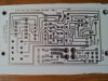
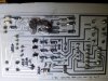
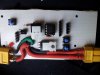
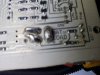
Having designed the PCB for my LiPo over-discharge protection circuit, it struck me that 40/80A is going to need quite a significant PCB trace to carry that much current. I checked on various trace width calculation sites and all came up with traces several centimetres wide, which does not seem unreasonable. HOWEVER, the Mosfet has a tiny leg that gets soldered into the track, that nowhere near matches the required trace thickness. It seems I am missing something here; why does the PCB trace need to be so much 'thicker' than the Mosfet leg?
I have now designed a PCB and kept the track to an absolute minimum length (5mm), but still envisage it going up in smoke.
What am I missing?
I have now designed a PCB and kept the track to an absolute minimum length (5mm), but still envisage it going up in smoke.
What am I missing?