Hello Guys,
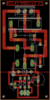
About a year ago I designed a simple one channel Relay Board PCB. I am about to manufacture couple of boards using PCBWay. So, I was wondering if you guys can check the PCB design and see if anything can be improved or any mistake was made in the design which needs to be corrected before manufacturing. Please help me out here so that I can proceed with the manufacturing. The relay specification is 250VAC@10A@50Hz. So, the relay module will also be used under that specification.
Link to full repo: https://github.com/uGiFarukh/Relay-Module
Thank You.