Maker Pro
Maker Pro

Multiple EPROMs in one large switchable-bank EPROM?

I just came across this rather interesting photo in a forum dedicated to an 80's EPROM based digital drum machine:
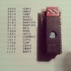
IMG_3438_2.JPG

Alas, there's not a whole lot of information available ther than this:

Anyone knows how many Chips uses the hihat sound on the LM1 ??? in my Linndrum are 4 2732
im tryin to get the LM1 sounds on my Linn but also using this new chip that a friend built to me , whiz is 16x a 2732.
just downloaded a file with the supposed LM1 sounds in bin format from here but there is only one bin file for the hihat also congas and toms , so I'm a little confused

here is a picture of the chip my friend built for me , with 16 switchable sounds
preety clever. but I'm figuring out how to get the longer sound without modify my linn, i thick i got it tho, but thats why i need to know how many chips are for the Hi Hat sound

Since I have another EPROM based drum machine (Oberheim DMX) containing voice cards with either 2732 (4K) or 2764 (8K) EPROMs and I sometimes swap these with other EPROMs (for other sounds) I was wondering....

Could an adapter board similar to the above be made, which plugs into the EPROM socket and contains a large EPROM of some sort which, by the help of DIP switches allow the voice card to see multiple 2732 or 2764 EPROMs? That would save me from swapping EPROMs all the time (a ZIF socket helps, but this would also eliminate having all those EPROMs around).
 

Harald Kapp

Moderator
Moderator
You could use a bigger EPROM (e.g. 27256) which has 4 times the capacity of a 2764. Tie the 2 most significant address bits (A14, A13) to pull-up resistors and a dip-switch to ground.
Connect the other pins (address, data, enable, power) to the respetive pins of a 2764 compatible socket.
Put the image of the first 2764 into the 1st 64 k of the 27256. Put the image of the 2nd 2764 into the 2nd 64 k of the 27256 etc.
By setting the DIP switch you can select on out of 4 images.

Use the three uppermost bits to emulate 2732 memory chips. 8 images of those will fit into one 27256.

This is very likely the same method used in the circuit in your image using a 27512 chip and the 4 uppermost address bits to select one out of 16 images from 2732 chips.
 
Excellent!
Here's a simple schematic I've made to see if I've understood correctly, with the different possibilities I have using different large EPROMs (27128, 27256 or 27512). The 2732 and 2764 pinouts are on the left (disregard the incomplete bus lines -the idea is to illustrate that the remaining address-lines, data-lines and power-lines join together):

eprom_adapter.png

So if I understand it correctly, with a 2732 I need to join together all the available address lines with the bigger EPROM (A0-A11) while the extra ones present only in the bigger EPROMs go to ground through a pullup resistor and the DIP switch?
If that's correct, the same should apply for the 2764 which joins together A0-A12 between the 2764 socket and the bigger EPROM, while anything from A13 and beyond goes through a pullup resistor and a DIP switch, right?

And I assume the D0-D7 pins are the same thing as O0-O7 which also join together between the 2732 (or 2764) socket and the bigger EPROM?
Should CE (chip enable) as well as OE (output enable) also be connected between the appropriate socket pins and the larger EPROM pins?

I think realistically I'll be using a 27256 in place of the 2732 socket and a 27512 in place of the 2764 socket which will allow for a total of 8 sound selections in both cases.
 
Last edited:

Harald Kapp

Moderator
Moderator
while the extra ones present only in the bigger EPROMs go to ground through a pullup resistor and the DIP switch?
In theory yes, but that is not what your schematic shows. Your resistors are pull-down, the pull-ups are missing.
upload_2018-7-13_13-40-48.png
 
You're absolutely right!
I've corrected it here and also improved the schematics, first for the 2732, next for the 2764:
2732_adapter.png
2764_adapter.png

Which values should the pullup resistors have?
 

Harald Kapp

Moderator
Moderator
That look good.
The values for the pull-ups are absolutely uncritical. Anything from 330 Ω to 10 kΩ should work, whatever you find in your parts bin.
 
Thanks Harald.
Another pleasant surprise I noticed by comparing datasheets is that the 2732 is pin-pin compatible with the 27256 by moving it down two pin-rows (except for one pin), so that should simpifly things.
A quick comparing between the 2764 and 27512 (both 28 pin) also shows an almost all pin-pin compatibility.
2732_27256 pinouts.png
 
A 27512 will most likely be used to replace the 2732, and a 27C010 for replacing the 2764. In both instances allowing 16 banks (i.e. 16 sounds) which means a 4-switch (16 position) DIP switch.

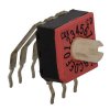
I see that rotary DIP switches are available, which would be more practical IMHO. I assume they work in a similar manner as regular DIP switches.
The datasheet in the above link lists different switch types: BCD, BCD-complement, hexadecimal, hexadecimal-complement. I think I saw some other types as well somewhere. Which type would be similar to the usual, rectangular DIP switches?
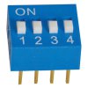
2277719.jpg 38820.jpg
 
Last edited:
Sorry for being a bit of a n00b. But I was wondering do those pull up resistors invert the data signal? (I could be completely off. I just never was told.) But they are just connected to switches, so maybe im wrong.

But I know you can actually invert with a single pole, just is restrictive to continue doing it.
 
I just realized that some of the address signals from the source (the voice board IC socket which takes a 2732 or 2764) are hardwired to a logic high state and wonder how I should redesign my multi-bank adapter for that?
Here's the information I came across (source: DMX files -1675 voice card configuration):

General information
The 1675 voice cards use one or two 2732 or 2764 EPROMs in various combinations. The EPROM sockets are pin compatible with 27128, 27256 and 27512 EPROMs, but only the top 4K or 8k bytes will be used - The 1675C card has EPROM address lines A15, A14 and A13 hardwired to a logic high state.
dmx24_28.jpg
2732 EPROMs have 24 pins instead of 28 pins, and must be inserted into the lower part of the IC socket, as illustrated above.

With a 27128, 27256 or 27512 inserted I find that logic high (VCC?) is connected to the following pins of the 28 pin socket:

pin 26 (A13)
pin 27 (A14)
pin 1 (A15)

And here's a comparison of all the signals coming from the IC socket (source), the 2732/2764 EPROMs (standard EPROMs used), 27128/27256/27512 EPROMs (plug-in compatible with the IC socket but only uses the topmost 4K or 8K, and finally the 27010 (or 27512) which will be plugged into new sockets on the multi-bank adapter board along with DIP switches and pull-up resistors (click image for bigger size):
DMX_source_signals.png

2732_adapter.png

2764_adapter.png
 
Last edited:
Thanks for confirming, Harald.
In post #2 you wrote that I should connect all signals (except for the uppermost MSB pins -in this case the 4 last address pins) to the DIP switch via pull-up resistors.

That's fine with the following pin signals:
Q0-Q7 (DMX IC socket) ----> Q0-Q7 (27010 or 27512)
OE (DMX IC socket) ----> OE (27010 or 27512)
CE (DMX IC socket) ----> CE (27010 or 27512)
GND (DMX IC socket) ----> GND (27010 or 27512)
VCC (DMX IC socket) ----> VCC (27010 or 27512)
A0-A12 (DMX IC socket) ----> A0-A12 (27010 or 27512)

PGM (27010) is missing from the DMX IC socket, so there's nowhere to connect this, but being "Program strobe"; should I just connect this to GND (possibly through a resistor)?

Finally there are the Most Significant Bits (MSB) pins (A13, A14, A15, A16 for the 27010 and A12, A13, A14, A15 for the 27512): A12 is available from the DMX IC socket (pin 2), so that's fine for connecting to the 27512, but for the other MSQ pins, they're all connected to VCC, so where do I connect those signals (on the 27010 and 27512) to? Do I need to redesign the schematic or the functionality will change (the order of the DIP switches)?
 
Last edited:

Harald Kapp

Moderator
Moderator
GM (27010) is missing from the DMX IC socket, so there's nowhere to connect this, but being "Program strobe"; should I just connect this to GND (possibly through a resistor)?
You can make this connection, but it will be dysfunctional. /PGMneeds to be strobed for programming, see the datasheet. In operation /PGM should beheld high.
Do I need to redesign the schematic or the functionality will change (the order of the DIP switches)?
I do not completely understand where you see a problem here. Look at the pinout, not the pinnumbers and everything matches as expected, or do I not get something here?
 
You can make this connection, but it will be dysfunctional. /PGMneeds to be strobed for programming, see the datasheet. In operation /PGM should beheld high.

Yes, I was worried about leaving the pin unconnected might cause its logic level to randomly fluctuate, or so I've heard can happen.
So connect PGM to VCC (high) then, in my circuit? (I'm guessing you mean in normal use by "in operation").

I do not completely understand where you see a problem here.

When I first posted here I didn't know that A13, A14 and A15 was hardwired to VSS (logic high), but now that I know -I'm worried that the circuit will function differently and not as intended, based on the new information available.
Does this mean that the 4 MSB signals are all logic high anyway, regardless of how that IC socket was wired?

Look at the pinout, not the pinnumbers and everything matches as expected, or do I not get something here?

Yes, I've been looking at the 2764 datasheet pinout as a source for where to take the signals to the 27010/27512 from, and for the mentioned MSB signals I looked at the 27128/27256/27512 pinouts (they're not present in the 2764).
Should I just stick to that and ignore what comes out of the DMX voice card IC socket?
Below is an updated schematic I've drawn:

2764_010_a.png
 

Harald Kapp

Moderator
Moderator
So connect PGM to VCC (high) then, in my circuit?
yes, this I meant.
hardwired to VSS (logic high)
Vss is logic low. Vcc (or Vdd) is logic high
Does this mean that the 4 MSB signals are all logic high
Yes, that is why only the upper memory area is being used.
Should I just stick to that and ignore what comes out of the DMX voice card IC socket?
Partly. Controlling A13 to A16 by the switches is why you need to "ignore" the hardwired Vcc from Pins 1, 27 and 28 and replace the switched address signals instead to select one of the different memory areas which are then addressed by A0 to A12 from the Socket.
 
Ah! Seems like I've over-complicated the circuit, thus confusing the matter even more :confused:

So the solution is very simple (as you already tried to explain before):
1) connect all the same signals (between the 2764 and 27010) together, REGARDLESS of how the DMX IC socket is connected
2) the four MSB signals (the unconnected 27010 pins) go to the DIP switch (with pullup resistors)

And I assume the 2732+27512 circuit is set up in the exact same way (the only difference being that the MSB signals are A12-A15). Do the two schematics (see below) make sense this time?
dmx2732_rev1.png

dmx2764_rev1.png
 
Top