Hi all,
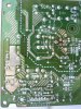
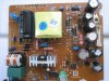
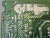
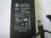
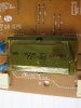
Got this LG Flatron L1942T-PF LCD monitor free from a friend but the problem is it does not have display power (power board model LGP-002L) and lacks a main transistor at Q101. After searching thru service manual, I installed a mosfet SSS7N60B at Q101, replaced all the secondary filter caps. Then I connect a 60W light bulb in series at F101,switched on mains 220vAC power,the light bulb flash a second,then lights off. This indicating there is no shorted component.
FYI, I have a digitalmultimeter(DMM), capacitor meter and a 40W soldering
iron with basic skills in replacing bulging capacitors and revive dead LCD monitors.
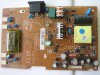
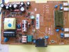
First,on the powerboard, I need to be sure there is poweroutput from P201 white connector where I perform DC voltage test by touching red probe to label 5V and black pin to cold ground (screw pad) but see no volt reading(zero volt) on DMM, meaning the 5V standby is not present.
Later on I perform the same DCvoltage test(red probe to cathode) on the following with the corresponding reading:
C101 main cap=286vDC
Q101(middle pin)=108VDC
D102 diode= -109vDC( negative reading?)
D107 diode=109vDC
D106=109vDC
D101=109vDC
D105 & D104= no DC at all
On power IC at U101 it is label LAF0001,pin 1=Vstr,pin 2=CS/FB,pin 5=Ground,pin 7=Vcc Putting my red probe to pin 7,black pin to cold ground yield a DC reading -109vDC(negative?)
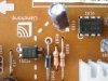
The opto at PC201 is label 817C,on diode test,one end on left facing D102 reads "1"= infinite while the other end reads 1335. Is the opto good?
Refer to inverter transformer at T301, I set my DMM to resistance test on 2k ohms scale. Reading on one end (1&2) is 1028 while pin 3&4 reads 1024. Guess the trans is good.
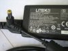
BTW, how do I test if the yellow transformer beside maincap is good with my limited DMM. I also attached some photos.
Hope someone can help me in solving the no power issue. Many thanks in advance.
Got this LG Flatron L1942T-PF LCD monitor free from a friend but the problem is it does not have display power (power board model LGP-002L) and lacks a main transistor at Q101. After searching thru service manual, I installed a mosfet SSS7N60B at Q101, replaced all the secondary filter caps. Then I connect a 60W light bulb in series at F101,switched on mains 220vAC power,the light bulb flash a second,then lights off. This indicating there is no shorted component.
FYI, I have a digitalmultimeter(DMM), capacitor meter and a 40W soldering
iron with basic skills in replacing bulging capacitors and revive dead LCD monitors.
First,on the powerboard, I need to be sure there is poweroutput from P201 white connector where I perform DC voltage test by touching red probe to label 5V and black pin to cold ground (screw pad) but see no volt reading(zero volt) on DMM, meaning the 5V standby is not present.
Later on I perform the same DCvoltage test(red probe to cathode) on the following with the corresponding reading:
C101 main cap=286vDC
Q101(middle pin)=108VDC
D102 diode= -109vDC( negative reading?)
D107 diode=109vDC
D106=109vDC
D101=109vDC
D105 & D104= no DC at all
On power IC at U101 it is label LAF0001,pin 1=Vstr,pin 2=CS/FB,pin 5=Ground,pin 7=Vcc Putting my red probe to pin 7,black pin to cold ground yield a DC reading -109vDC(negative?)
The opto at PC201 is label 817C,on diode test,one end on left facing D102 reads "1"= infinite while the other end reads 1335. Is the opto good?
Refer to inverter transformer at T301, I set my DMM to resistance test on 2k ohms scale. Reading on one end (1&2) is 1028 while pin 3&4 reads 1024. Guess the trans is good.
BTW, how do I test if the yellow transformer beside maincap is good with my limited DMM. I also attached some photos.
Hope someone can help me in solving the no power issue. Many thanks in advance.
Attachments

Last edited by a moderator:


")