.
Sir Constantine . . . . . . .
Is it possible that the PCB does not use R802 ?
I would expect it to be placed to the side, just as the R801 is now located.
Minor issue, since it's JUST being a s l o w drain after power off, for those massive E-caps.
I will check again but i am confident that it is not a soldering issue.
Not soldering, since the transistor goes into PCB holes, BUT possibly you inverted that parts installation, a full 180 degrees.
Looking ahead for the next troubleshooting step:
Referring to ADOBE schematic page 39:
You see that the LEFT channels schematic has all of its parts well marked up but you have to figure out the
companion parts if working on the other RIGHT channel.
ALSO they have the audio flow shown as a grey defined path for the LEFT channel.
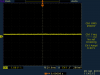
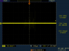
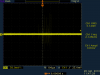
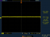
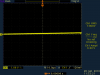
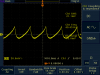
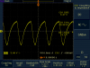
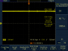
What we want to ascertain, is if this HIGH level signal on the RIGHT channel; as is being confirmed by your frequency analyzer display . . . .by its FULL bars UP on the extreme right bar display.
Now . . .Is that signal being generated within the final power output stage . . . .or is it just coming into that stage.
To determine if it is an incoming signal:
Look at schema connector P-701 coming into the Power stage.
Its pin 2 would serve as a good shared common ground connection and the RIGHT audio coming into the
stage would be on pin 7.
Take a 0.1 through 1 ufd capacitor and connect between pin 2 and 7 and see if the unwanted signal at the display either disappears or diminishes in amplitude, if using the 0.1 value.
That then should show if an incoming signal . . . .which I can't imagine the origin of THAT freq of signal . . .or is it being created within the output stage circuitry ?
And you do have some SPECIAL little devices, in the form of those IC751 and 752's.
But we could inter swap them, if it comes down to that .
That's enough for now, until seeing the testing results.
73's de Edd
Sir Constantine . . . . . . .
Is it possible that the PCB does not use R802 ?
I would expect it to be placed to the side, just as the R801 is now located.
Minor issue, since it's JUST being a s l o w drain after power off, for those massive E-caps.
I will check again but i am confident that it is not a soldering issue.
Not soldering, since the transistor goes into PCB holes, BUT possibly you inverted that parts installation, a full 180 degrees.
Looking ahead for the next troubleshooting step:
Referring to ADOBE schematic page 39:
You see that the LEFT channels schematic has all of its parts well marked up but you have to figure out the
companion parts if working on the other RIGHT channel.
ALSO they have the audio flow shown as a grey defined path for the LEFT channel.
What we want to ascertain, is if this HIGH level signal on the RIGHT channel; as is being confirmed by your frequency analyzer display . . . .by its FULL bars UP on the extreme right bar display.
Now . . .Is that signal being generated within the final power output stage . . . .or is it just coming into that stage.
To determine if it is an incoming signal:
Look at schema connector P-701 coming into the Power stage.
Its pin 2 would serve as a good shared common ground connection and the RIGHT audio coming into the
stage would be on pin 7.
Take a 0.1 through 1 ufd capacitor and connect between pin 2 and 7 and see if the unwanted signal at the display either disappears or diminishes in amplitude, if using the 0.1 value.
That then should show if an incoming signal . . . .which I can't imagine the origin of THAT freq of signal . . .or is it being created within the output stage circuitry ?
And you do have some SPECIAL little devices, in the form of those IC751 and 752's.
But we could inter swap them, if it comes down to that .
That's enough for now, until seeing the testing results.
73's de Edd