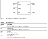
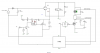
Your schematic doesn't show supply voltages where it would be appropriate. This will make reading and understanding the schematic much easier.
He does not.
This is the voltage for the 1EDN751x, right? This is good enough for the MOSFET chosen.
There's no "best way". What's best always depends on the application. In your simple motor drive application you don't need separate control of turn-on and turn-off, therefore the "driver 1" configuration with a single output pin will suffice.
The MOSFET datasheet states a total input capacitance of typ. 9820 pF- Make that 10 nF. This capacitance together with the gate resistor forms an RC low pass filter. Compute the rise time of the gate voltage after the RC filter such that the MOSFET turns on sufficiently fast, taking into account the output rise (and fall) time of the driver. Make sure not to exceed the max. output current of the driver (4 A high, -8 A low).
A quick back of the envelope calculation:
Assuming turn on with Vgs = 0V and Vout = 12 V and a max. current of 4 A gives R = 12 V / 4 A = 3 Ω
The driver output resistance is between 0.4 Ω and 1.5 Ω. Worst case here is least resistance, therefore the external gate drive resistor should be at least 2.6 Ω for a conservative design. The time constant of the RC element is tau = 3 Ω * 10 nF = 30 ns. After approx. 3*tau = 100 ns the gate voltage has reached 12 V. But note that the MOSFET will turn on for Vgs=4 V (max.) which is reached after approx. 15 ns - imho sufficiently fast for this application as the driver itself has a 10 ns rise time.
Note that this is really a rough approximation. A detailed description how to select a proper gate drive resistor for MOSFETs using the EiceDriver is given in this
application note.
Thank you.
I will change to the 2EDN driver which has two drivers instead of one. Of course I will just use one, the other will be useless. The reason is because the 1EDN drivers are not available. Seems like they are out of production. I mean, according to the datasheet, the 1EDN has two versions:
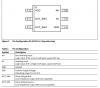
z=7: lower voltage for logic level MOSFETs (typ. 4.2 V)
z=8: higher voltage for standard and superjunction MOSFETs (typ. 8.0 V)
The Z=7 is the only one available, but my mosfet is not logic level. So I chose an ULVO of 8 which is only available at the 2EDN series.
This is the datasheet for the 2EDN driver:
https://www.infineon.com/dgdl/Infin...N.pdf?fileId=5546d462525dbac40152abcc7dbb1727
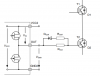
Also, for the gate resistor calculation, I think I have to take into account the gate resistance of the MOSFET, which according to table 5 of the datasheet is 1.3 ohms.
I saw the app note about gate resistors for power devices, but for the gate resistor calculation I need the charging and discharging peak current, which is where I'm confused. For example,
The gate driver power supply is 12V.
The sink/source capability of the driver is 5A.
So taking into account the worst scenario where the charging current is equal to the peak current of the driver (5A)
RGon = 12/5 - (0.55 + 1.3) = 0.55 ohms
where 0.55 ohms is the Rds(on) or source resistor of the driver and 1.3 ohms is the mosfet gate resistance.
For the discharge current
ROff = 12/5 -(0.7 + 1.3) = 0.4 ohms
where 0.7 ohms is the sink resistance of the driver.
It's supossed that the charging peak current has to be less than driver peak current (5A). So, how do I know the real charging peak current?
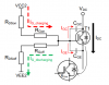
In the Gate2.PNG picture attached, do I need the diode and the discharging resistor?
Additional info: I plan to use a 25kHz frequency for the PWM (could be lower)