Well, you're doing OK for a 13-year-old! If you put your date of birth in your profile, we will see your age, and will be able to respond accordingly.
It can also help if we know your location, so we know what component suppliers to recommend.
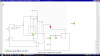
OK, that circuit has a number of problems and can be simplified a great deal.
First, let's get the schematic issues out of the way.
1. The power rails.
You have shown the 0V rail across the bottom, which is good. It's also customary to put the supply voltage (the batteries, in this case) at one end or the other.
Each IC should have its own decoupling capacitor connected between its power and 0V terminals as close as possible to the device. Typically a 0.1 µF ceramic capacitor is used.
2. Component identification
"D1" should be "Q1" because it's a phototransistor, not a photodiode.
"OP1" should really be "IC1" or "U1" because it's an IC. Sure, it's an op-amp, but an op-amp is just a type of IC, and you don't call the CD4001 "NOR1".
The 4001 should have its VDD and VSS connections (pins 14 and 7) shown.
The op-amp and the 4001 should have all of their pin numbers marked, and you should show the unused sections. The inputs of the other half of the LM358 can be tied to VDD, and unused CMOS inputs should be tied either high or low otherwise they pick up noise and increase power consumption.
It's better to show all part numbers on the schematic, next to the components. Having a separate list wastes time and leads to errors ("OP1" vs. "OP", and the CD4001 "U1" is also marked IC2a on the schematic).
We know what a "358P" is, but you should show the full name, which is normally LM358P or LM358N.
Now to the design issues.
I'm going to address them all, even though I'm going to suggest changes that will make most of them irrelevant. This is supposed to help you learn. Let me know if you don't want detailed explanations.
3. Two +3.6V rails.
You seem to have two +3.6V rails. One from BT1 supplies "D1" and Q2, and the other supplies OP1 and Q1. I don't see any need for two separate batteries.
4. D1 needs a load resistor.
"D1" (which is not a diode) passes an amount of current that depends on the light level falling on it. An op-amp or comparator compares voltages. You need to convert the current into a voltage. This is what resistors do.
If you add a resistor between the emitter of "D1" and 0V, the current that flows through R1 and "D1" will cause a proportional voltage drop across the resistor. That voltage can then be fed into an input of an op-amp, comparator, or other circuit.
Say you want the resistor voltage to be around half supply (1.8V) when the light falling on "D1" causes a current flow of, say, 500 µA. Rearrange Ohm's Law to give R = V / I and plug in the numbers:
R = V / I
= 1.8 / 500 x 10
-6
= 3600 ohms
= 3k6.
There is no need for R1 because the maximum current that can flow through "D1" will be limited by the load resistance and the power supply voltage.
There is also no need for Q1 because op-amps, comparators and most voltage-input circuits have a fairly high input resistance, so buffering isn't needed.
If you want the dark/light threshold to be adjustable, you can use a trimpot - 10k for example. In this case you might want to protect "D1" from excess current if the trimpot happens to be turned to minimum resistance and "D1" is exposed to lots of light. You could put R1 back in the collector path, or in series with the trimpot (better). R1 doesn't need to be so high though; to limit the current to 10 mA from a 3.6V source, R = 360 ohms.
5. OP1 has one input tied to its output and the other input tied to VDD.
You can't tie the output of an op-amp back to the input where the input signal is being applied. Q1 and the op-amp output will fight and the voltage will not be properly defined.
The only time you connect an op-amp's output back to its input like that is when you're making a buffer or voltage follower. In that case, the output connects back to the inverting ('-') input, not the non-inverting ('+') input, and the input signal is applied to the non-inverting ('+') input. The op-amp then acts as a buffer.
Most op-amps and comparators won't do anything useful if one of the inputs is tied to the device's VCC pin. Op-amps and comparators only work over a limited range of input voltages. Many will work with their inputs tied to their negative supply rails (these are called "single supply" devices), and one or two will work with their inputs tied to their positive supply rails (but not the LM358).
The change you need to make here depends on what you're intending to do with the op-amp. If you want to use it as a comparator, you need to set one of the inputs to a threshold voltage. Often this voltage is created using a voltage divider (two resistors in series) across the supply rails.
If you intend to use the op-amp as a voltage follower (buffer), connect the output to the inverting input. But there's no need for a buffer; the inputs of a CMOS gate have much higher impedance than the inputs of an LM358 have!
6. Threshold voltage, CD4001 gate, hysteresis
The voltage you get from the phototransistor reflects a real-world quantity, and these aren't usually clean and tidy. A phototransistor responds quicker than the human eye, and it will see the flicker of fluorescent and incandescent lights, and can detect very small variations.
If you want a clean ON/OFF control from this signal, you need to clean it up. This is why I mentioned hysteresis.
You seem to understand what hysteresis is, and why it's needed. If not, say so and I will explain.
The CD4001 inputs don't have hysteresis. Worse than that, around the decision voltage the gate goes into "linear mode" where it draws extra current from the supply. This is not recommended. You can get CMOS devices that have hysteresis built in - the CD4093 quad NAND gate and the CD40106 (aka CD4584 and 74C14) hex inverters.
Does Yenka know about any of those devices? If so, they are a reasonable choice for this circuit. If not, it's not hard to make a Schmitt trigger with two transistors and three resistors - see
http://www.physics.ucdavis.edu/Classes/Physics116/Schmitt_fig.GIF
7. LED drive from emitter follower
You have Q2 connected as an emitter follower. This is a good buffer circuit, but it wastes voltage - about 0.7V base-emitter voltage. This means less voltage for LED D2. A better option is a PNP common emitter circuit. That is a PNP transistor, with its emitter connected to the positive rail, its base connected to the Schmitt trigger output through a resistor (e.g. 1k), and its collector feeding the LED.
If D2 actually represents a real LED, you'll also need a current limiting resistor in series with it. If it represents the Christmas lights string, that's designed to be powered straight from a battery, then you don't use a current limiting resistor.
Have a think about all that, and let me know how you want to proceed.


")


