Learn how to to realize a low-side sensing over current detection circuit with a latching output.
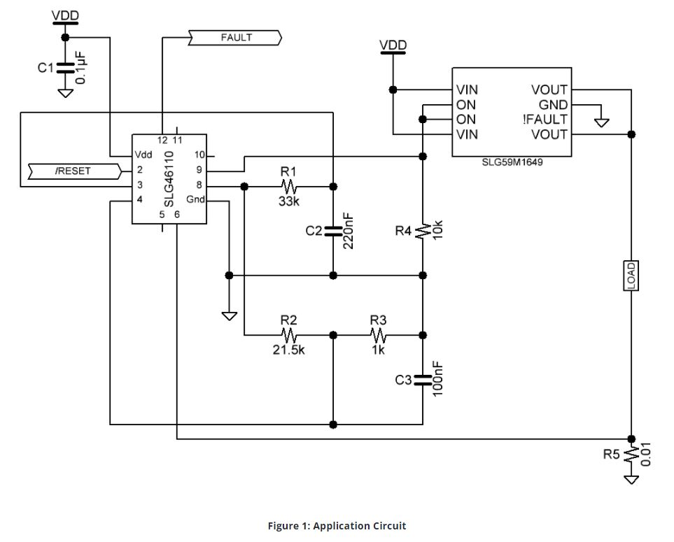
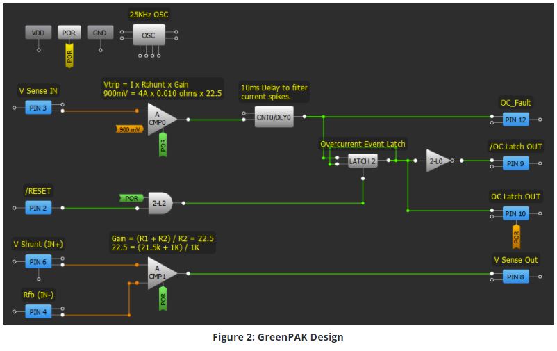
This design uses a single GreenPAK™ SLG46110V to realize a low-side sensing over current detection circuit with a latching output used to enable/disable an external high-side PMOS load switch. By configuring one of the onboard comparators (ACMP1) to perform as a non-inverting amplifier with a gain of 22.5, we can use a very small 0.010 Ω low-side sense resistor to, in this case, detect a 4 A maximum current. Figure 1 shows the full circuit schematic while Figure 2 shows the internal design of the SLG46110V GreenPAK circuit.
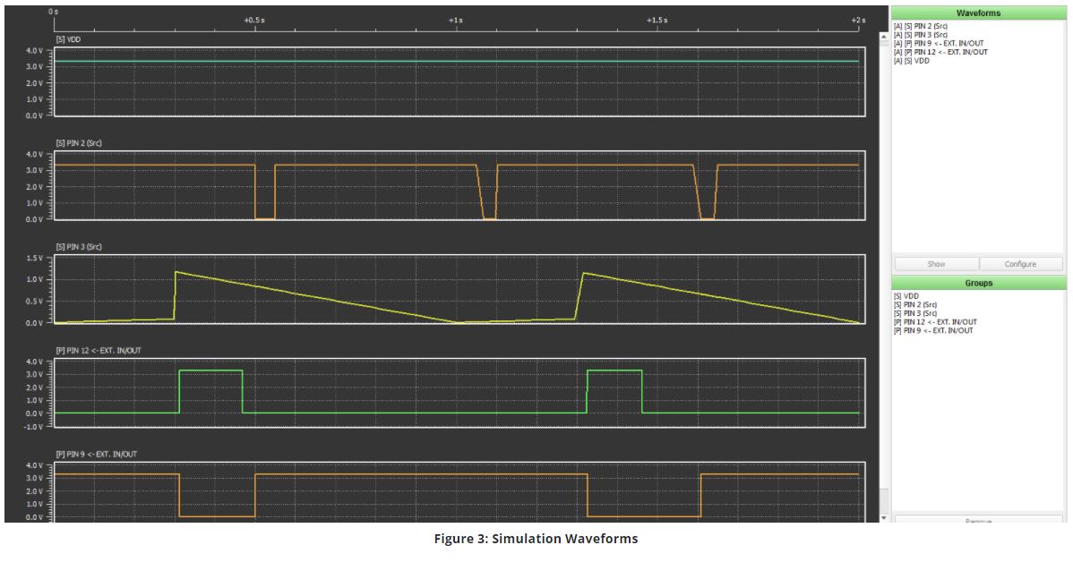
The circuit functions as follows and the associated simulation waveforms are given in Figure 3. Once the 4 A limit is exceeded (shown by the yellow trace), the output of ACMP0 will trip HIGH, setting both the output of Latch 2 and the OC_FAULT output HIGH (shown by the green trace). The /OC_LATCH_OUT and OC_LATCH_OUT outputs are tied to the output of Latch 2, so when the Latch 2 output goes HIGH, the /OC_LATCH_OUT output goes LOW and turns OFF the load switch. Once tripped, the /OC_LATCH_OUT output on Pin 9 will remain LOW, even if the overcurrent event is gone, keeping the external load switch turned OFF. If the overcurrent condition is now cleared, the output of ACMP0 will go LOW, thus the OC_FAULT output will now go LOW, as it follows the output state of ACMP0. However, the /OC_LATCH_OUT output will remain latched LOW. In this event, the micro can now look at the OC_FAULT signal, determine that the over current event has been corrected, and send a LOW going pulse to the /RESET input on Pin 2 (shown by the orange trace). The low going pulse on the /RESET input will then reset the output of Latch 2 to LOW, and thus set the /OC_LATCH _OUT output HIGH, thereby turning on the external switch.
All essential parameters in the design are customizable to the needs of the application. The gain associated with ACMP1, the voltage trip level associated with ACMP0, signal polarities, load switch and sense resistor can all be configured to match the requirements needed. With the unused resources within the SLG46110V, additional features can also be added to enhance the circuit functionality. One example would be to add an “automatic retry” circuit that would automatically clear the /OC_LATCH_OUT signal after a set period of time. If the continued over current situation caused another immediate trip, the circuit would initiate another retry. It would continue to attempt to clear the /OC_LATCH_OUT signal for a preprogrammed number of times, and if unsuccessful, it would finally latch the /OC_LATCH_OUT signal LOW. At this point the external switch would be latched off until the fault is cleared and a low going pulse is input on Pin 2, /RESET.
This circuit provides a small, configurable, low cost solution for overcurrent safety functions. With the addition of a few properly selected external passive components, this solution can cover a wide range of overcurrent applications needing electronic circuit breaker functions.
The complete design file can be found here. It was created in the GreenPAK Designer software (a part of the Go Configure™ Software Hub).
Configuring GreenPAK Comparators as OpAmps
Often when using a GreenPAK device there is a need to add gain to an input signal in order to bring it into a measurable range for use by the ADC or the comparators. In some GreenPAK devices there is a PGA available to perform this function. The PGA is quite versatile in its configurability but the input voltage range is limited and its gain is limited to a maximum setting of x8. The SLG46110V has no internal Operational Amplifiers (OpAmps). As a result, it would be nice to have a way of incorporating some gain into your GreenPAK design without adding extra OpAmps.
One method to achieve this would be to try and adapt one of the onboard comparators for use as an OpAmp. This is something that has been done for years in highly integrated solutions where cost and size were major factors. With a bit of work and a few external R’s and C’s you can effectively make a low power OpAmp from a spare comparator in your GreenPAK design. This is by no means a high speed, high performance OpAmp solution but for many applications where gain is needed on the input signal from a sensor, we are only looking to amplify a slow-moving DC signal. For many applications such as these where we are measuring temperature or voltage across a shunt resistor, a solution such as this is more than adequate.
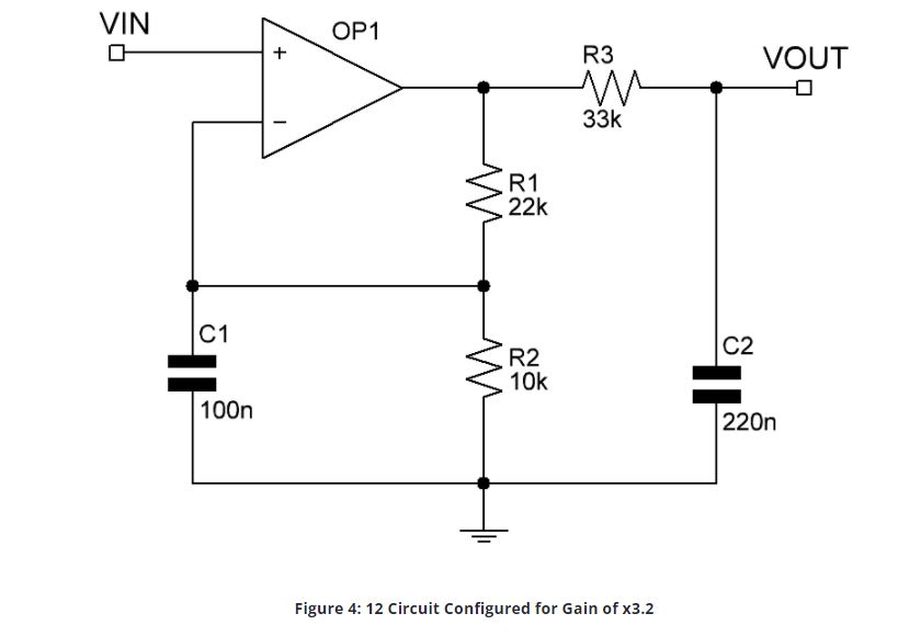
In order to configure one of the comparators for use as an OpAmp, we first look at the overall circuit, shown in Figure 4. The comparator is configured as a non-inverting OpAmp with VIN being connected to the non-inverting input of the comparator. The inverting input of the comparator is connected to the center point of the resistive divider made up of R1 and R2, with C1 adding a bit of RC time constant to the feedback signal. The resistor, R3, in combination with C2, will act as a low pass filter, in this case yielding a 24 Hz cutoff. VOUT is then the voltage across C2.
The circuit functions as follows. When the voltage across C1 is less than the input voltage at VIN, the output of the comparator is HIGH. This causes the voltage across C1 to rise. Once the voltage across C1 is greater than VIN, the output of the comparator switches LOW. Now the voltage across C1 begins to fall until it is less than VIN, at which point the output of the comparator switches HIGH and the cycle begins again. After many cycles the filtered average voltage seen across the output capacitor, C2, is given by the transfer function of the non-inverting amplifier.
VOUT = VIN (R1 + R2) / R2
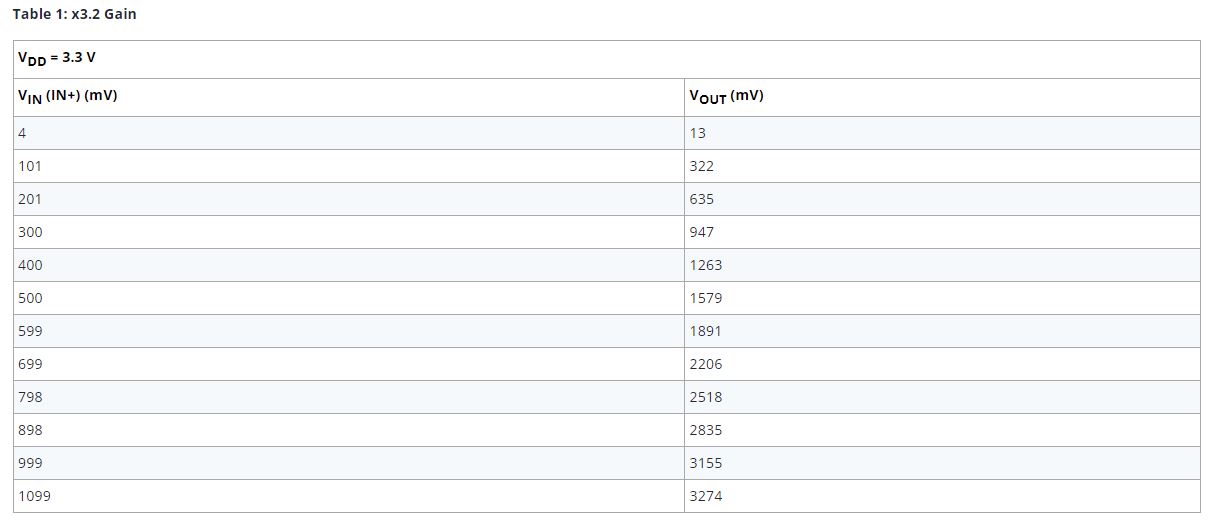
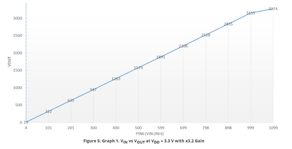
The circuit in Figure 4 was tested and measured yielding results very close to the calculated gain of x3.2. A table of measured data is given in Table 1 along with the associated data plot for VOUT vs. VIN at VDD = 3.3 V.
As shown in Figure 5, there is some error at both extremes of the plot when the input is near 0 V and when the output is near the 3.3 V rail. There is an offset present at the low end of the VOUT vs. VIN plot. This offset can be easily calibrated out of the system, if necessary, but that is not the focus of this project. Techniques for correcting OpAmp offsets are readily available on the internet. At the high end of the plot, as we get close to the VDD rail, the gain becomes slightly nonlinear. This is to be expected and illustrates the need to allow a bit of headroom below the VDD rail and limit the output swing of the circuit to around VDD – 300 mV or about 3.0 V max. with a VDD of 3.3 V.
One additional limitation of this circuit is the input voltage range. The IN+ node at VIN can normally take a voltage up to VDD but the IN- node is limited to about 1.2 V. For example, a 1.5 V VIN signal with the OpAmp configured for a gain of 2 and VDD = 3.3 V, will cause the circuit to exceed the input voltage range of the IN- node. Once IN- is above 1.3 V, it will cause the output to go to the rail until VIN is brought back down below 1.2 V. So, as a rule, it is recommended to limit the VIN range to 0 < VIN < 1.2 V, max.
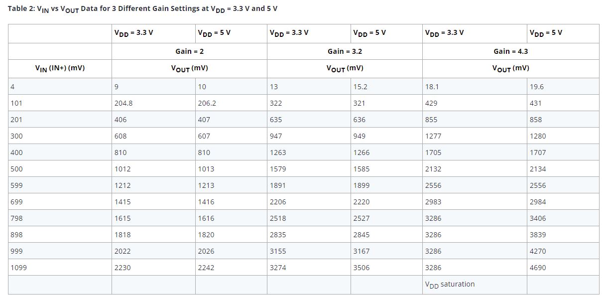
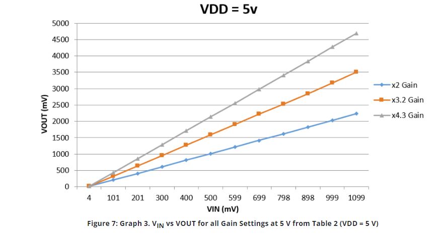
Additional VIN vs VOUT data at various gains was taken for both VDD = 3.3 V and VDD = 5 V. That data is listed in Table 2 and plotted in Figure 6 and Figure 7. In all cases the output is very linear within the VIN < 1.1 V and VOUT < VDD – 300 mV constraints.
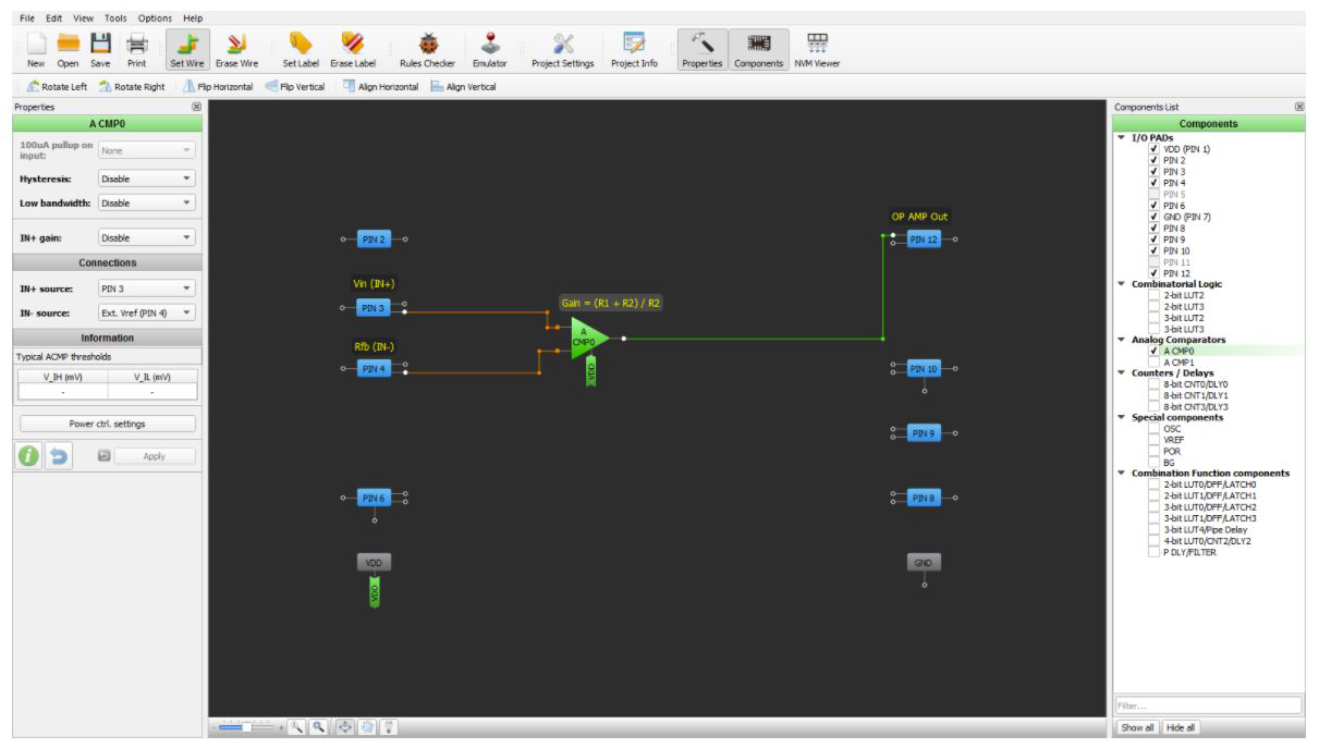
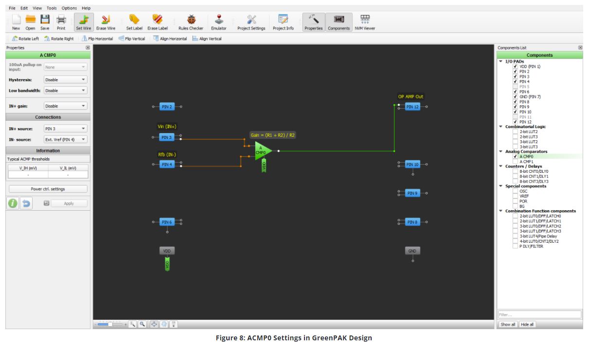
Figure 8 is a screenshot of the circuit designed into an SLG46110V. The figure shows not only the circuit but also the remaining resources and pins that are available to add other features and perform other functions. The actual GreenPAK design program file is attached as well.
Based on the analysis given, the circuit operates quite well and as expected. The gain is very linear and accurate for VOUT < VDD - 300 mV and VIN < 1.1 V. For many slow varying DC signals this performance is more than acceptable for adding some needed gain and enables the designer to now measure and compare these signal values more accurately and easily without adding additional external OpAmps.