Learn about KiCad, an open-source PCB layout software suite used by hobbyists and professionals alike.
KiCad is a free package available for designing circuits and PCBs. Its software integrates schematic capture, custom symbols and libraries, PCB design, calculators, and useful tools all in one package and is available for Windows, Mac, and Linux.
Thanks to its popularity and open source nature, KiCad is continually developing with the latest versions incorporating many thousands of components and complex features such as microwave traces and multilayer PCBs.
Installing KiCad on Windows is very easy—a single executable installer is all that is needed. Installing KiCad onto Linux distros such as Ubuntu can be done either through software managers or the terminal and is too somewhat simple. While all the instructions and demonstrations in this article are on a Windows system they should be identical for other systems.
KiCad's Main Window
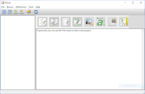
When you open KiCad, you are presented with a window similar to the one shown below.
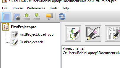
In order to use the various tools and programs you need to either create or open a project. This is done by clicking File > New Project > New Project or by clicking the New Project icon on the top left of the window.
Creating a new project in KiCad.
When a new project is created you will notice that the window on the left (which shows all project files), will have two new files: a schematic file and a PCB file.
KiCad schematic files have the extension “.sch” and PCB files have the extension “.kicad_pcb” and the creation of schematic files often results in KiCad automatically generating the PCB file for that schematic file.
KiCad has two file types: schematic (.sch) and PCB (.kicad_pcb).
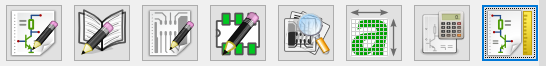
Along the top of the middle window are the buttons that launch the various inbuilt applications. In order of appearance these applications are:
- eeschema – The schematic editing program
- Schematic library editor – For making new libraries
- Pcbnew – The PCB editing program
- PCB Footprint editor – For creating new PCB footprints
- GerbView – Gerber viewer
- Bitmap2Component – Convert an image into a PCB component (logos e.g.)
- PcbCalculator - Calculator program for various applications
- PI Editor – For creating custom sheets
KiCad's application toolbar
KiCad's Design Flow
When creating a KiCad project you follow a specific design flow which is somewhat similar (if not identical) to most other programs.
eeschema
The first stage involves the creation of the schematic using the eeschema program. When the components have been placed and wired together, they are assigned part numbers which can be done either manually or automatically using optional numbering schemes. With the parts numbered, a component file is produced which includes a list of all the parts as well as a netlist of how they connect together.
CvPCB
A special program is then launched form eeschema called CvPCB which is used to select PCB footprints for each component (such as a DIP40 for a large PIC chip or a 7.92mm resistor outline for a standard 1/4W resistor). With the footprints chosen the PCB program is then loaded and the netlist imported. The components are positioned, oriented, and the routed to result in the final PCB. While KiCad does not come with an autorouter there is a free autorouter available that does a surprisingly good job.
GerbView
The PCB can from there be converted into gerber files which are checked using GerbView and then sent to a production house. The PCB editor also contains tools such as design rule checkers so trace widths and clearances can be checked which are vital when designing PCBs.
An Introduction to an Important Design Resource
This introductory article only looks at the main window of KiCad and the inbuilt tools to get you started. Later articles will look at each tool in more depth.
Despite being free, KiCad is a very powerful circuit creation tool and is more than capable of being used in professional environments (the author would argue that KiCad is better than many commercially available packages). With the capability of 16 layers, all PCB footprints, no limitations on PCB size, thousands of pre-made components, and the many thousands of free libraries online, KiCad is one of the biggest players in open source circuit design and worth familiarizing yourself with!