Learn how to add more design elements to your custom image in this series on custom PCB art design!
Our bitmap import is complete!
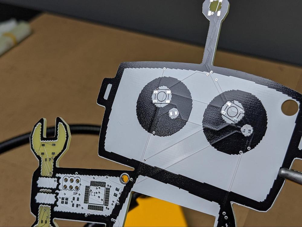
Now that we have an outline of the Maker Pro robot PCB in the Dimension layer in Eagle, the next step is adding the internal design elements: the black outline around the outside of the design, the robot’s eyes, the small light on the antenna, and other details.
In order to accomplish this, we need to use a couple of different layers in Autodesk Eagle because each will be a different color in the finished PCB.
Different Colors on the PCB
One of the major skills in creating artistic PCBs is mastering techniques for creating different colors on the PCB.
Normally, colors are (more or less) inconsequential for PCB designs. Usually, PCBs are embedded into some part of the enclosure so the user will never see it. Therefore, the color of the PCB, or for that matter, the general aesthetics of the board, matters very little, if at all.
It is a very different story with PCB art and PCB badges where color plays a central role in the design. By making use of different layers in Eagle, we can create different colors for the different parts of the design.
For a normal PCB design, there are four colors available:
- Solder mask
- Silkscreen layer
- Bare copper areas
- Bare FR4
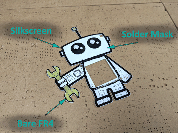
The different layers of our PCB
Solder Mask
The solder mask color is the default color for any area of the PCB not occupied by pads, the silkscreen layer, components, or certain other specialized layers. Many PCB manufacturers allow different solder mask colors to be specified as part of their ordering process. In this project, we will use a white solder mask.
Silkscreen Layer
The silkscreen layer is the second most common color on a typical PCB. Normally the silkscreen is used to show information for positioning components, component identifiers, and other text used for assembly.
For PCB art, we can make use of the silkscreen layer to create internal design elements. For most PCB manufacturers, the silkscreen is white unless the solder mask is white, in which case the silkscreen is typically black. This is the case with the Maker Pro robot PCB.
Bare Copper Areas
It is possible to create bare copper areas on the PCB using design elements on both the top/bottom layer and the tStop/bStop layer.
Basically, a shape is created on the top or bottom layers which creates a copper area in the PCB design. Then, by copying the shape onto the tStop or bStop layer, the solder mask can be kept away from the shape. This creates an area of bare copper on the board, a technique that is uncommon for normal PCB design work but it highly useful for artistic PCBs.
The color of the bare copper area depends upon the surface finish chosen for manufacturing. For this project, we will be using a HASL lead-free finish. Because this finish is close to white, we will not be using this technique for this tutorial.
Bare FR4
Last, similarly to bare copper areas, design elements can be created in bare FR4, the substrate material used for PCBs. To pull this off, shapes are drawn on the tStop or bStop layers. Bare FR4 areas are yellow in color. We will use this technique for the Maker Pro robot’s wrench.
Create a Bitmap from the Design Graphic
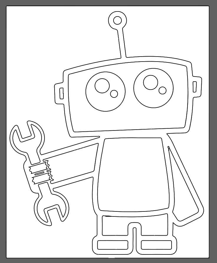
To get started, open the file you saved earlier that has the full image trace in Illustrator. It should look something like the image below.
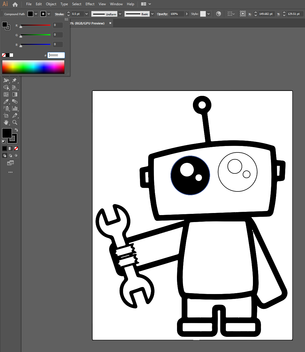
Then, we need to add black fill to the areas that will show up on the PCB.
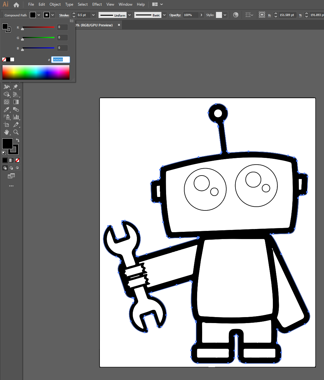
Start by clicking on the outline of the design the same way you did for isolating the outline from the rest of the graphic. In the Appearance toolbar, hold SHIFT and click the left-most color selection box. Then choose black as the fill color, which will fill in the entire border area inside the outline.
Next up is adding fill to the eyes, which needs to be done one eye at a time. Select the outline of one of the eyes and again hold SHIFT and click the left-most color selection button in the Appearance toolbar. Choose a black fill color. Then repeat for the other eye.
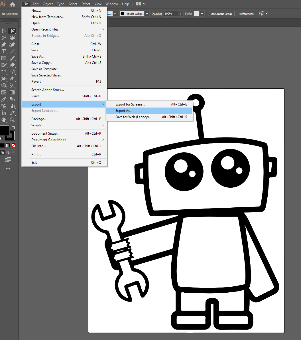
With both eyes and the outline filled in, we will work on exporting the image from Illustrator and import it into Eagle. From the File menu, select Export > Export As…
Export this image from Illustrator
In the Export dialog box, give your file a name and choose BMP (*.BMP) as the file format.
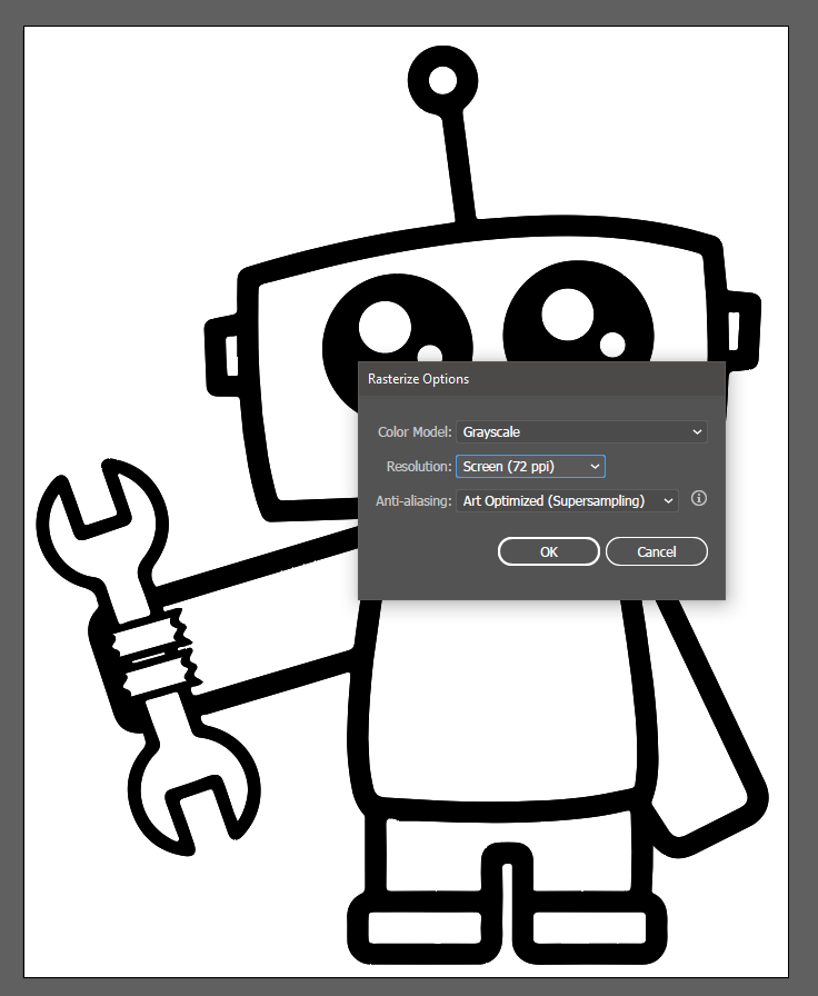
Looking ahead slightly, the ultimate goal here is to export the border/eyes elements of the design as a bitmap image. The bitmap can then be imported into Eagle. However, the bitmap import feature in Eagle is limited to images with a minimal pallet of colors (4-8 bit color if you want to get technical). Therefore, we need to set the exported image to grayscale only.
In the Rasterize Options dialog box, select Grayscale from the Color Model dropdown menu. The Resolution setting will also be very important for moving the image into Eagle. It should be set to Screen (72 ppi).
Export the image in grayscale
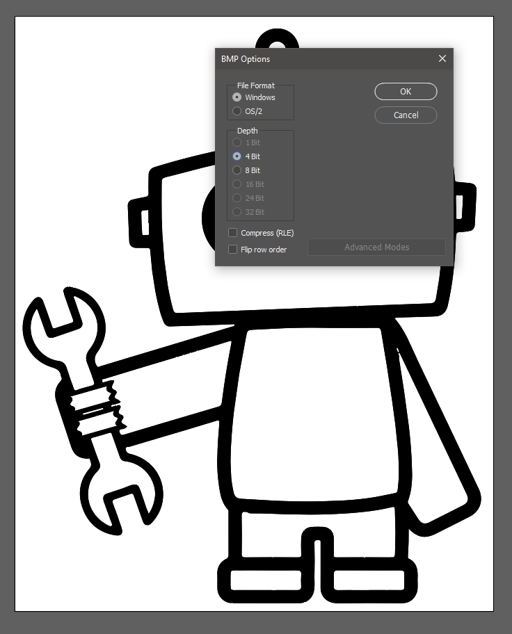
Then we will get yet another dialog box. In the BMP Options dialog box, select 4 Bit from the Depth setting. Finally, click the OK button to save the BMP image.
Selected settings for exporting as a bitmap file
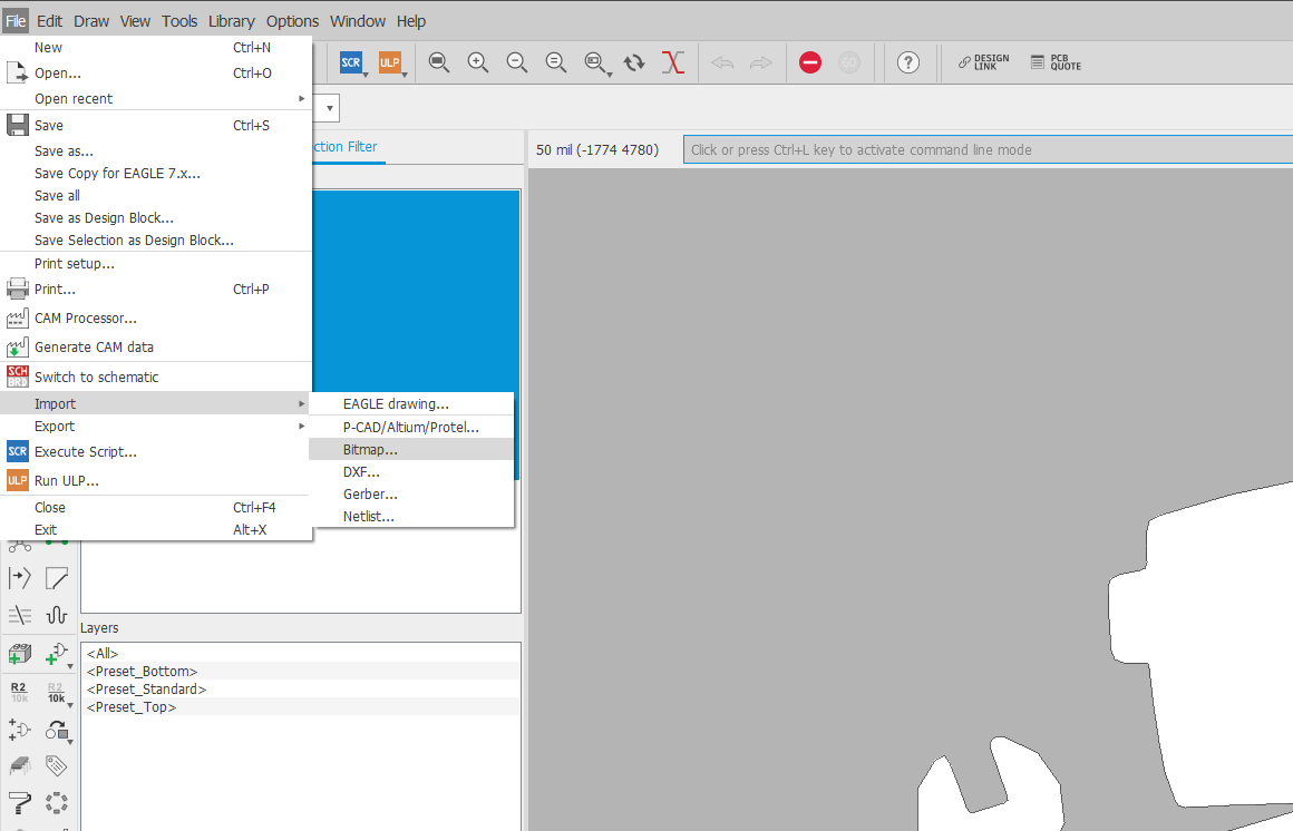
Import the Bitmap into Eagle
Now, jump back over to Eagle and open the board file with the PCB outline on it. To import the bitmap we just created with Illustrator, select File > Import > Bitmap.
Import the newly-created bitmap in Eagle
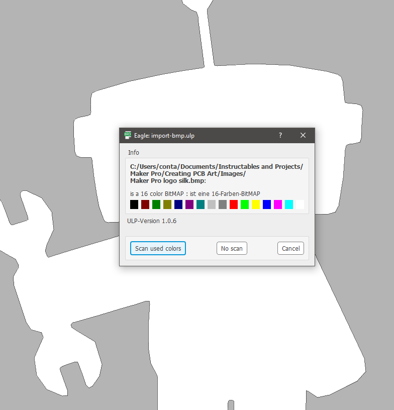
After finding and selecting the bitmap from Illustrator, Eagle will present what might be a slightly confusing dialog box. It will have a row of colored squares on it. This function basically scans the colors in the image so that you can select which areas of the bitmap should be imported into Eagle. In this case, there is only one color of interest, black. So, click the No Scan button.
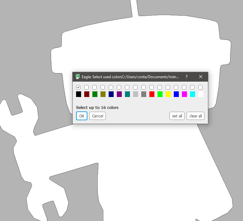
Then you will be presented with a similarly-designed dialog box, but this time there will be a checkbox above each of the colored squares. Check the black square and click OK.
Ccheck the black box and click OK
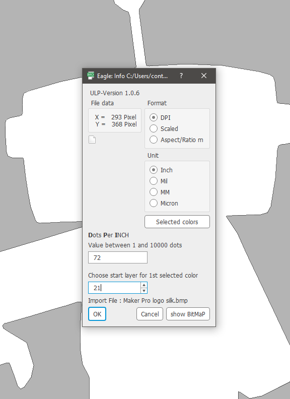
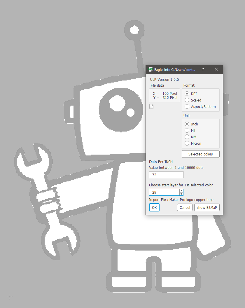
Next up is another dialog box containing the settings for importing the bitmap.
First, we need to select the type of scaling to use for the import. From the Format area, select DPI. Second, in the Dots Per Inch field, enter 72. This value matches the DPI value chosen while exporting the bitmap from Illustrator. This value is how the imported bitmap will end up the correct size in the PCB design file. Third, in the Choose the start layer for the 1st selected color field, enter 21. Layer 21 is the tPlace layer.
When you have all of this filled out, press OK.
Required selections for the type of scaling dialog box.
Last, you will be presented with a dialog with a script in it. The bitmap import function works by generating a script to translate the image into a layer in Eagle. Just click the Run script button to finish the import.
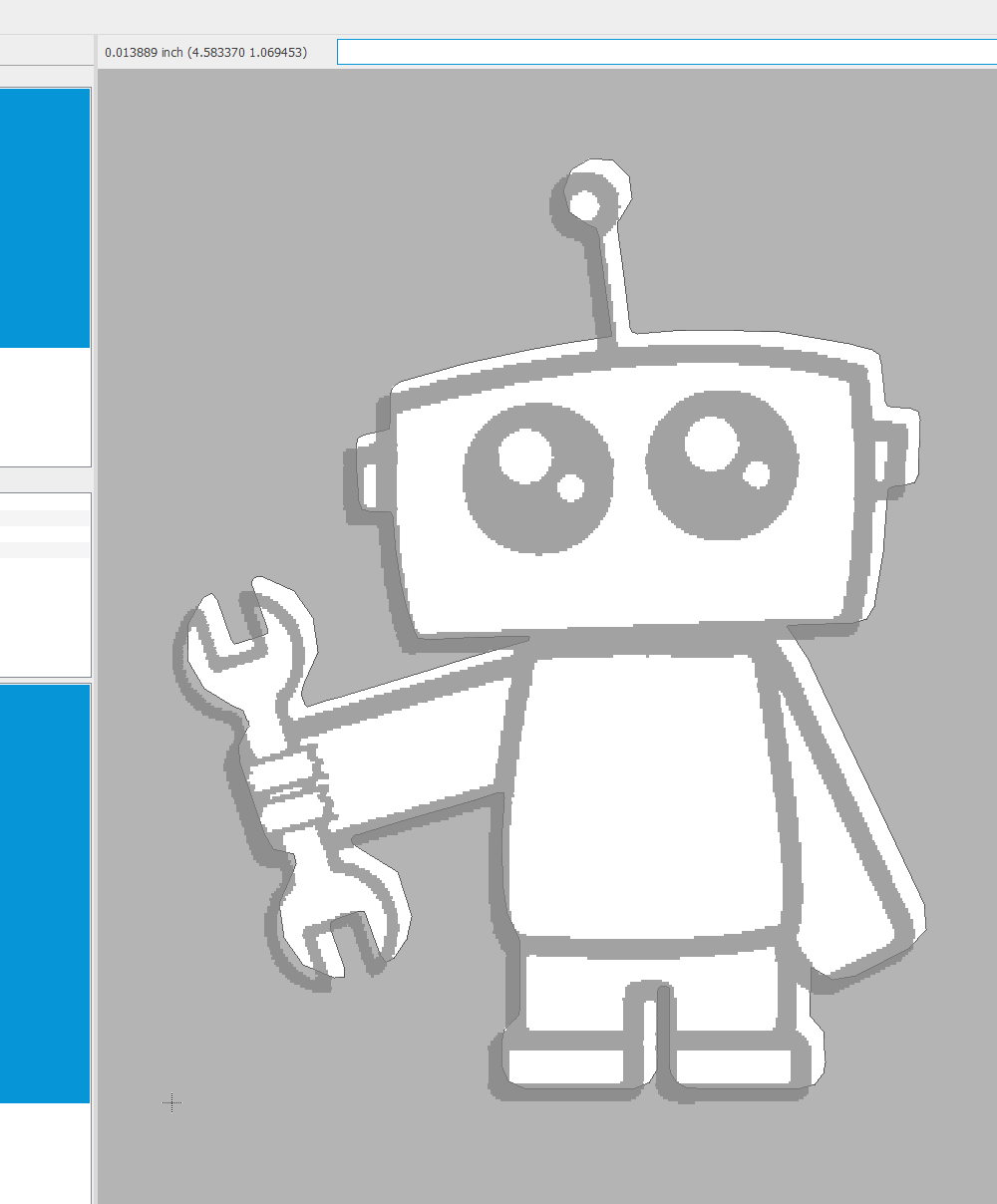
Our bitmap import is complete!
However, as you can see, the imported image is not quite in the correct spot. We’ll have to move it.
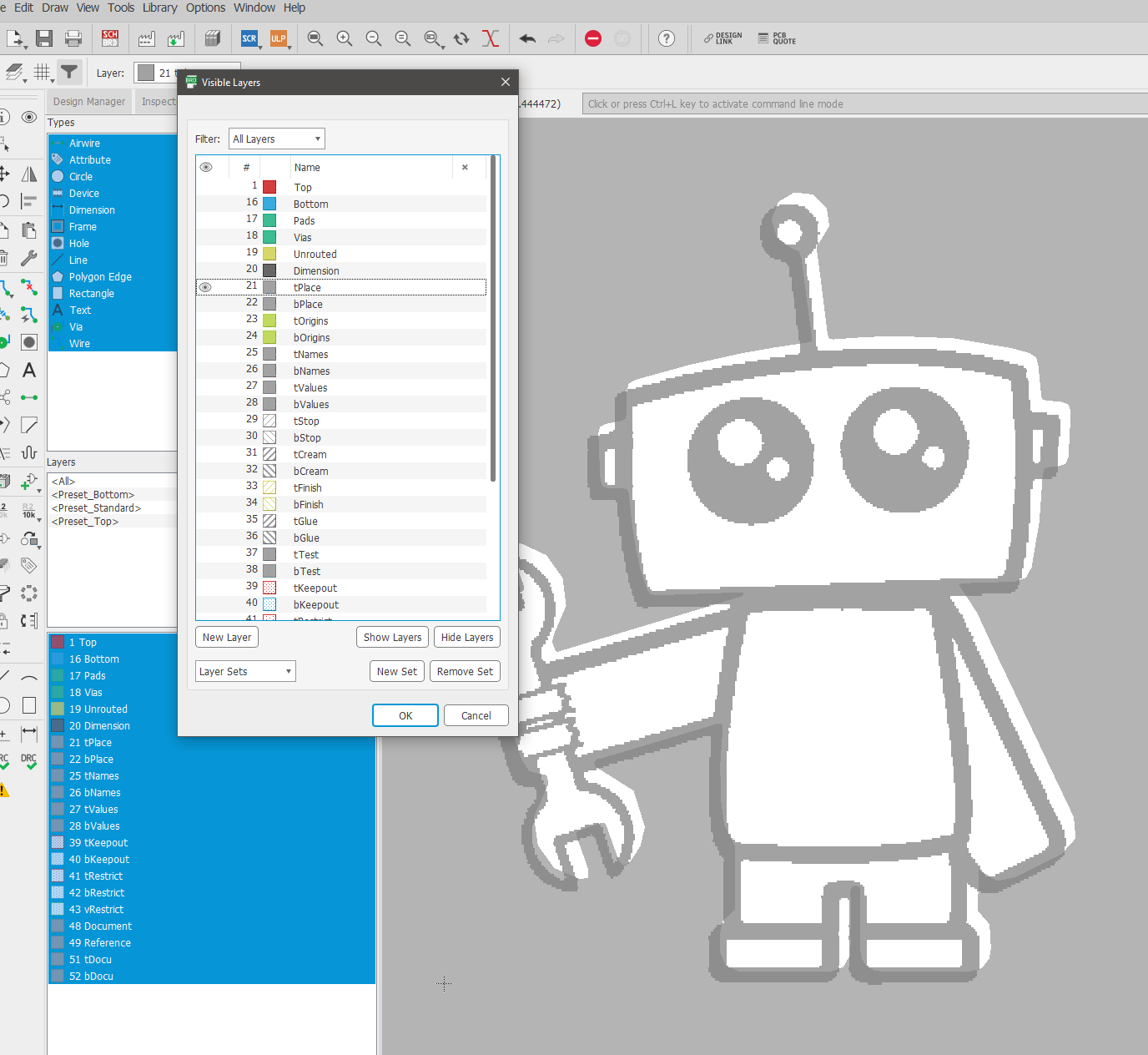
In order to move only the imported image and not any other part of the design, we will turn off all the layers except layer 21. Open Layer settings, then press Hide layers to disable all the layers and turn on only layer 21.
Using the Group tool, select the entire design. Then, with the Move tool, right-click and select Move Group. Carefully reposition the imported bitmap so that it lines up with the outline.
Carefully adjust the bitmap so that it lines up with our original image
Adding Bare FR4 Areas
In the Maker Pro robot PCB design, we’ve used two different colors so far: the solder mask is white and the silkscreen is black.
For the robot’s wrench and the light at the top of the antenna, we will use bare FR4 as another color. The process for creating bare FR4 areas in Eagle is very similar to the process of creating graphics in the previous section.
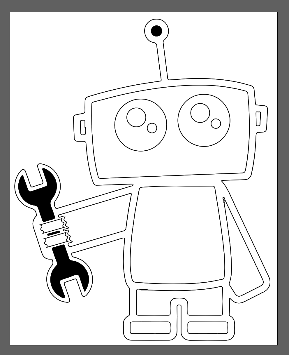
We again start with the graphic containing the entire Maker Pro robot image trace. This time, using the Group Selection Tool, start by selecting the light at the top of the antenna. Then, as we did before, hold SHIFT and click on the far left box in the Appearances toolbar. Select black as the fill color for the top of the antenna.
Choosing the fill color for the robot’s antenna.
Then, use the same procedure to fill in the wrench in black. There are three sections to the wrench: the top, the bottom, and the small section between the fingers.
Choosing the fill color for the wrench
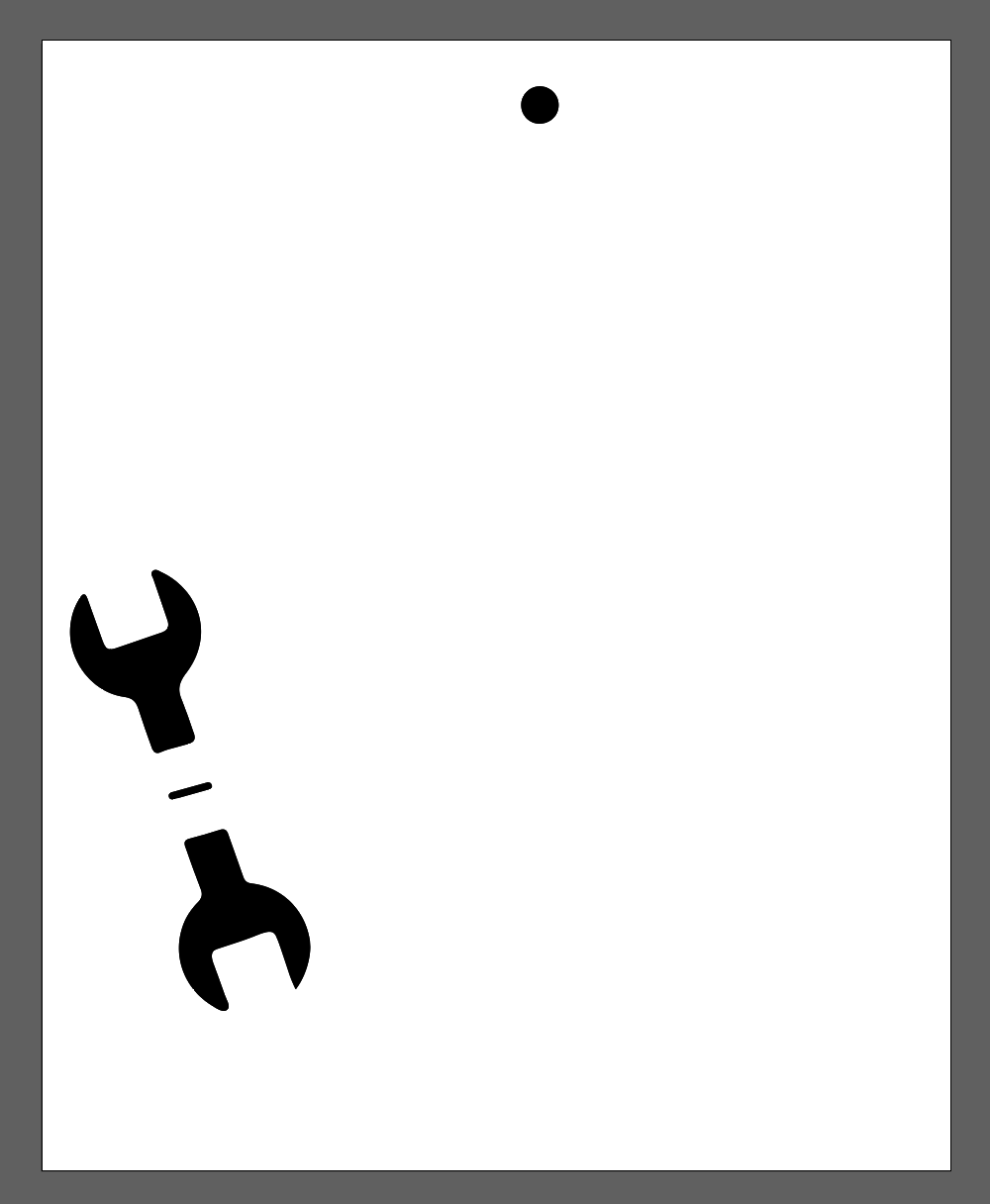
In this case, we do not need the outline, so select the outline and delete it. You will be left with only the top of the antenna and the wrench, both filled in with black.
What we're left with after deleting the outline.
With the prep work done, export the image as a bitmap using exactly the same procedure as the previous section.
Importing the bitmap into Eagle will also use the same steps as before, except for the layer onto which the bitmap will be imported. This time, we will import the bitmap onto the tStop layer, which is layer 29.
Import the antenna and wrench bitmap as level 29
As before, after the import script completes, the design will not be in quite the right place. Using the group selection and move tools, reposition the bitmap so that it lines up with the other parts of the design.
Reposition the antenna and wrench bitmap to align the other layers
A Review of the PCB Color Process and Next Steps
One of the unique skills involved in creating artistic PCBs is using different PCB layers to create different colors on the PCB:
- The solder mask color is specified when you manufacture the PCB.
- Likewise, the silkscreen layer is typically white or black, as specified during manufacturing.
- We will not be using it in this tutorial, but it is possible to create bare copper areas on the PCB, the color of which depends upon the surface finish chosen for manufacturing.
- Bare FR4 areas are yellow in color.
In this step, we used bitmaps to create internal design elements in the PCB. The outline of the robot and the eyes are black on the silkscreen layer. The antenna and wrench are bare FR4.
At this point, we are done with most of the non-traditional work of translating the reference image into a PCB design in Autodesk Eagle. In this next part of this series, we will go back to basics and create an electrical schematic for the project.