Learn about the open-source design program Fritzing, which offers circuit design, schematics, and PCB layout to Makers.
One of the most important aspects of creating new projects is the initial design and vetting process to figure out whether your circuit will work or not. Fritzing is a free, open-source design tool that provides users with circuit design, schematics, and PCB layout creation. This article serves as an introductory overview of what Fritzing has to offer.
What is Fritzing?
Fritzing is a free design program that can be used to design circuits on breadboards, create schematics, and even develop PCBs. Unlike a lot of other circuit design suites, Fritzing is polished and heavily uses vectorized images, producing beautiful looking circuits.
While Fritzing includes many popular components such as the Arduino range of boards and modules, it is geared for hobby and maker use rather than professional use. Along with the free design features, there is also a community forum and a projects page where users can upload their projects.
Designing a Project on a Breadboard
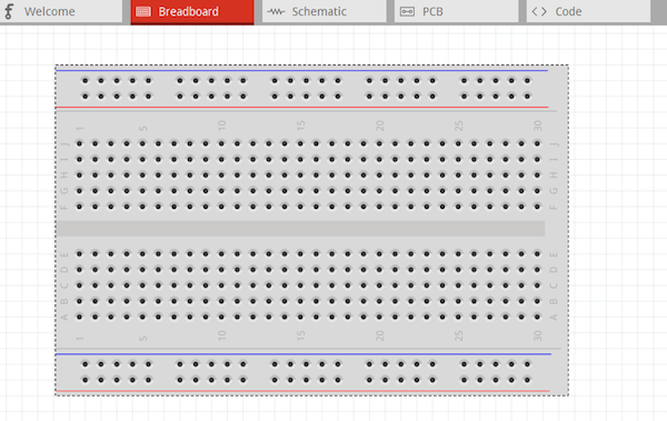
The first main window in the Fritzing environment is the breadboard view which allows the creation of breadboard circuits. The breadboard size can be adjusted, and the set up is interactive, allowing users to drop components and wires to individual pins.
Breadboard view in Fritzing.
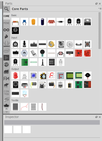
The window on the right-hand side of the screen allows the user to find and place a variety of components onto the breadboard and a search makes finding specific parts easier.
Component pick and place window.
Unlike more advanced circuit suites (such as KiCad), the list of parts available is limited to the most commonly used modules and microcontrollers (for example, there are plenty of Arduino boards but no PIC devices).
Parts from the search window are dragged into the breadboard area and should snap into holes as the legs cross them. When a part is dropped into place, the rows that are electrically connected to that component’s legs show up. This helps to make identifying rows easier, and wires placement clearer. Wires can be made by click and holding— they are also snapped to holes on the breadboard.
Creating wire placements on a breadboard.
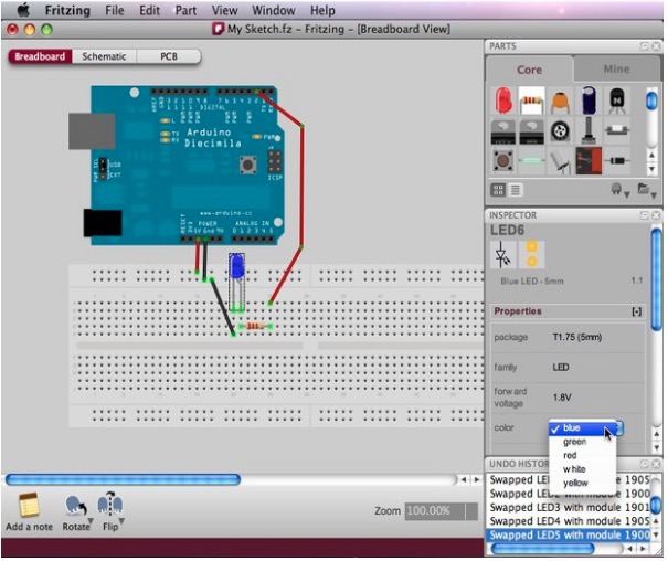
Users can select wires and change their color as needed. Changing the color of wires is very good practice with designs that heavily rely on wires.
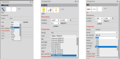
The inspector window, which is directly below the component search window, can be used to edit components including the breadboard.
Inspector windows in Fritzing.
When the options above are applied to our simple LED circuit we can see that the LED is now yellow, the wires color-coded red (for power), and black (for ground), and the resistor is set to 1K. A battery was also included as a source of power.
Color-coded circuit design.
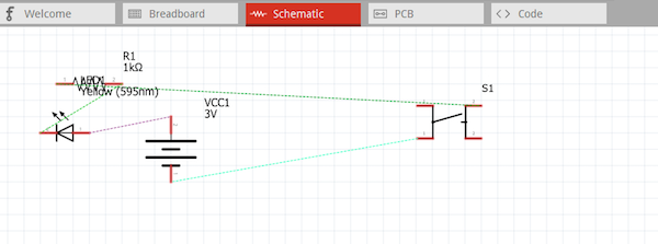
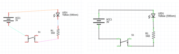
Converting Circuits Into Schematics
Once a circuit is created on the breadboard, it can then be converted into a schematic. One of the really cool features in Fritzing is that as you construct your breadboard circuit, it automatically adds parts into the schematic and forms connections between those parts according to their placement on the breadboard. The schematic, however, will not be neat or complete and requires some rearranging of the components to form the connections.
The schematic window in Fritzing.
Dotted lines indicate connections between components. Components can be dragged around by clicking and holding. Parts are easily rotated by clicking the part and the pressing Ctrl + R. Wires can be added by clicking the dotted lines.
Dotted lines in schematic view indicate connections between components.
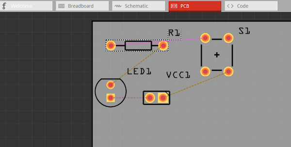
Creating PCB Layouts
The PCB layout is the last stage of creating a circuit in Fritzing. Like the schematic stage, the parts on the PCB are automatically placed on the board. Again, the user is required to orient and position these components.
The PCB stage is optional because not every project is going to use a PCB. One of the major advantages of using Fritzing is that the software works in conjunction with the Fritzing PCB service which easily turns a design on Fritzing into a low-cost PCB.
The PCB design window in Fritzing.
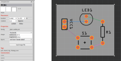
Just like in the schematic layout, components and their neighboring indents can be dragged and rotated. The PCB itself can also be easily resized by dragging the corners. The inspector window provides additional options such as the number of layers on the PCB and the specific shape (such as an Arduino shield shape).
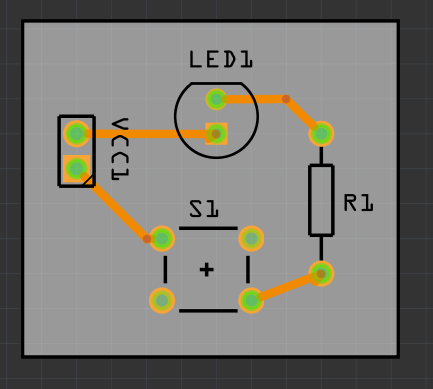
In the example below, the PCB has been shrunk down and set to be a single-sided PCB so that there are only copper traces on the underside.
A single-sided PCB design alongside its settings in the Inspector window.
Copper tracks can be routed either by double-clicking the dotted line or clicking and dragging from the pads. If manual routing proves too difficult, Fritzing also comes with a simple auto-router that can route your PCBs automatically.
Orange lines represent copper traces in the PCB design window.
Have you ever used Fritzing? What are your favorite features? Let us know in the comments!
Cover image courtesy of Fritzing.