This project describes how to build a smart digital dimmer using GreenPAK™ SLG46620V.
This project describes how to build a smart digital dimmer. A dimmer is a common light switch that is used in houses, hotels, and many other buildings. Older versions of dimmer switches were manual, and would typically incorporate a rotary switch (potentiometer) or buttons to control the light level. This project describes how to build a digital dimmer that has two ways of controlling light intensity; a smartphone and physical buttons. The two modes can work seamlessly together so that the user can increase or decrease luminosity from both a button and smartphone. The project is implemented using an SLG46620V IC, HC-06 Bluetooth module, pushbuttons, and LEDs.
We are going to use the SLG46620V IC as it helps minimize discrete project components. GreenPAK™ ICs are small and have multiuse components, which allows a designer to decrease components and add new features. Additionally, the project cost is subsequently reduced.
The SLG46620V also contains an SPI connection interface, PWM blocks, FSM, and a lot of useful additional blocks in one tiny chip. These components allow a user to build a practical smart dimmer that can be controlled via a Bluetooth device or wall buttons, support extended-time dimming, and the addition of selectable features without using a microcontroller or expensive components.
Project features:
- Two methods of control; mobile app and real buttons.
- Smooth on-off transition for the light. This is healthier for a consumer’s eyes. It also gives a more luxurious feeling, which is appealing to hotels and other service industries.
- Sleep mode feature. This will be an added value for this application. When the user activates this mode, light brightness decreases gradually in 10 minutes. This helps people who suffer from insomnia. It is also useful for kids’ bedrooms and retail shops (closing time).
Project Interface
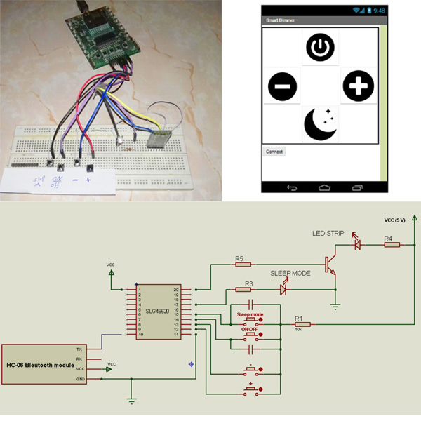
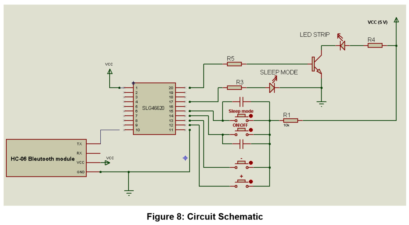
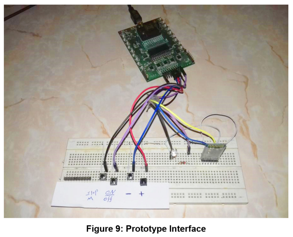
The project interface has four pushbuttons, which are used as GreenPAK inputs:
ON\OFF: turn the light ON\OFF (soft-start\stop).
UP: increase light level.
Down: decrease light level.
Sleep Mode: by activating sleep mode, light brightness decreases gradually over a period of 10 minutes. This gives the user time before sleeping and guarantees that the light will not stay ON all night.
The system will output a PWM signal, which will be passed to an external LED and sleep mode LED indicator.
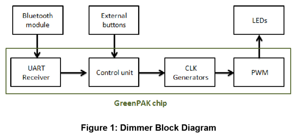
The GreenPAK design is comprised of 4 main blocks. The first is a UART receiver, which receives data from the Bluetooth module, extracts orders, and sends them to a control unit. The second block is a control unit, which receives orders coming from the UART receiver or from the external buttons. The control unit decides the required action (Turn ON/OFF, Increase, decrease, enable sleep mode). This unit is implemented using LUTs.
The third block supplies the CLK generators. In this project, an FSM counter is used to control the PWM. The FSM's value will change (up, down) according to the orders given by 3 frequencies (high, medium, and low). In this section, the three frequencies will be generated and the required CLK passes to FSM according to the required order; In turning on/off operation, high frequency passes to FSM to soft start/stop. During dimming, the medium frequency passes. The low frequency passes in sleep mode to reduce the FSM value more slowly. Then, light brightness decreases slowly too. The fourth block is the PWM unit, which generates pulses to external LEDs.
The complete design file can be found here. It was created in the GreenPAK Designer software (a part of the Go Configure™ Software Hub).
1. GreenPAK Design
The best way to build a dimmer using GreenPAK is by using the 8-bit FSM and a PWM. In the SLG46620, FSM1 contains 8 bits and can be used with PWM1 and PWM2. The Bluetooth module must be connected, which means the SPI parallel output must be used. The SPI parallel output bits 0 through 7 connections are muxed with DCMP1, DMCP2, and LF OSC CLK, OUT1, OUT0 OSC outputs. PWM0 obtains its output from FSM0 (16 bits). FSM0 does not stop at 255; it increases up to 16383. To limit the counter value at 8 bits another FSM is added; FSM1 is used as a pointer to know when the counter reaches 0 or 255. FSM0 was used to generate the PWM pulse. As the two FSM's values must be changed at the same time to have the same value, the design becomes a bit complex where in both FSMs have a predefined, limited, selectable CLK. CNT1 and CNT3 are used as mediators to pass the CLK to both FSMs.
The design consists of the following sections.
1.1. UART Receiver
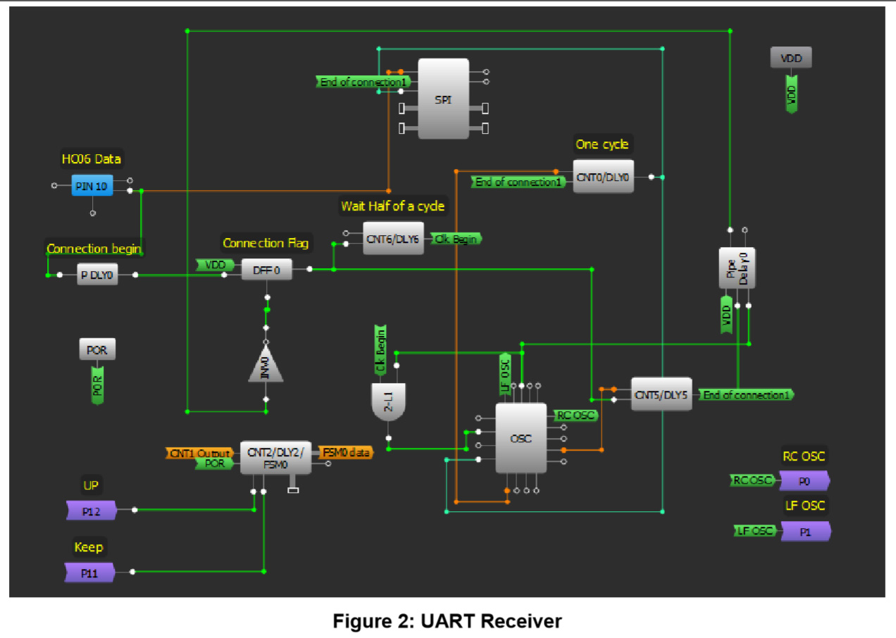
First, we need to set up the HC06 Bluetooth module. The HC06 uses the UART protocol for communication. UART stands for Universal Asynchronous Receiver / Transmitter. UART can convert data back and forth between parallel and serial formats. It includes a serial to parallel receiver and a parallel to serial converter which are both clocked separately. The data received in the HC06 will be transmitted to our GreenPAK device. The idle state for Pin 10 is HIGH. Every character sent begins with a logic LOW start bit, followed by a configurable number of data bits, and one or more logic HIGH stop bits.
The HC06 sends 1 START bit, 8 data bits, and one STOP bit. Its default baud rate is 9600. We will send the data byte from the HC06 to the GreenPAK SLG46620V’s SPI block.
Since the GreenPAK SPI block does not have START or STOP bit control, those bits are instead used to enable and disable the SPI clock signal (SCLK). When Pin 10 goes LOW, the IC has received a START bit, so we use the PDLY falling edge detector to identify the start of communication. That falling edge detector clocks DFF0, which enables the SCLK signal to clock the SPI block.
Our baud rate is 9600 bits per second, so our SCLK period needs to be 1/9600 = 104 µs. Therefore, we set the OSC frequency to 2 MHz and used CNT0 as a frequency divider.
2 MHz-1 = 0.5 µs
(104 µs / 0.5 µs) - 1 = 207
Therefore, we want the CNT0 counter value to be 207. To ensure that data is not missed, a half clock cycle delay on the SPI clock is added so that the SPI block is being clocked at the proper time. This is accomplished by using CNT6, 2-bit LUT1, and the OSC block’s External Clock. The output of CNT6 does not go high until 52 µs after DFF0 is clocked, which is exactly half of our SCLK period of 104 µs. When it goes high, the 2-bit LUT1 AND gate allows the 2 MHz OSC signal to pass into the EXT. CLK0 input, whose output is connected to CNT0.
1.2. Control Unit
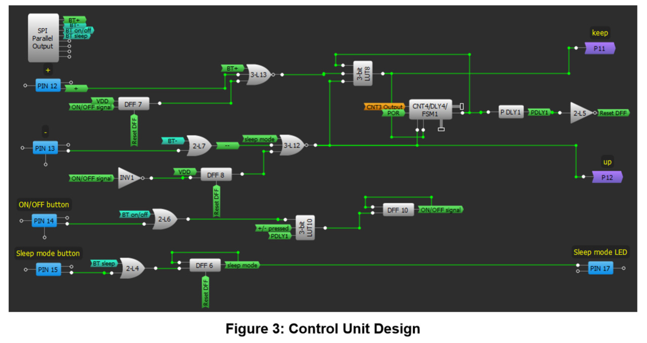
In this section, commands will be executed according to the received byte from the UART receiver, or according to the signals from the external buttons. Pins 12, 13, 14, 15 are initialized as inputs and are connected to external buttons.
Each pin is internally connected to an OR gate input, while the second input of the gate is connected with the corresponding signal that coming from the smart phone via Bluetooth which is going to appear on SPI Parallel output.
DFF6 is used to activate sleep mode where its output changes to high with the rising edge coming from 2-bit LUT4, while DFF10 is used to maintain the lighting status, and its output changes from low to high and vice versa with every rising edge coming from 3-bit LUT10 output.
FSM1 is an 8-bit counter; it gives a high pulse on its output when its value reaches to 0 or 255. Consequently, it’s used to prevent FSM0 (16-bit) from exceeding the value 255, as its output resets DFFs and it changes DFF10 status from on to off and vice versa if lighting is controlled by the buttons +, - and the maximum/minimum level has been reached.
The signals connected to FSM1 inputs keep, up will reach FSM0 through P11 and P12 to synchronize and keep the same value on both counters.
1.3. CLK Generators and Multiplexer
In this section, three frequencies will be generated, but only one will clock the FSMs at any one time. The first frequency is RC OSC, which is fetched from the matrix 0 through P0. The second frequency is LF OSC which is also fetched from the matrix 0 through P1; the third frequency is the CNT7 output.
3-bit LUT9 and 3-bit LUT11 allow one frequency to pass, according to the 3-bit LUT14 output. After that, the chosen clock transmits to FSM0 and FSM1 through CNT1 and CNT3.
1.4. PWM
Finally, FSM0 value transforms to PWM signal to appear through pin 20 which is initialized as an output and it is connected to the external LEDs.
2. Android app
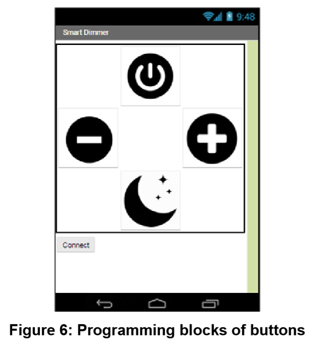
The Android app has a virtual control interface similar to the real interface. It has five buttons; ON\OFF, UP, DOWN, Sleep mode, and Connect. This Android Application will be able to convert button presses into a command and will send the commands to the Bluetooth module to be carried out.
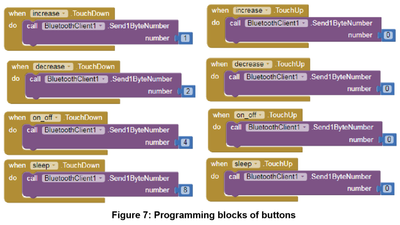
This app was made with MIT App Inventor, which doesn’t require any programming experience. The App Inventor lets the developer create an application for Android OS devices using a web browser by connecting programming blocks. You can import our App into the MIT App Inventor by clicking on Projects -> Import project (.aia) from my computer, and selecting the .aia file included with this project.
To create the Android Application a new project must be started. Five buttons are required: one is a list picker for Bluetooth devices, and the others are the control buttons. We need to add a Bluetooth client as well. Figure 6 is a screen capture of our Android Application’s user interface.
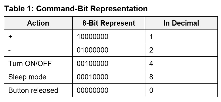
After we add the buttons, we are going to assign a software function for each button. We are going to use 4 bits to represent the status of the buttons. One bit for each button, therefore, when you press the button, a specific number will be sent via Bluetooth to the physical circuit.
These numbers are shown in Table 1:
Conclusion
This project describes a smart dimmer that can be controlled in two ways; an Android app and real buttons. Four separate blocks are outlined within the GreenPAK SLG46620V which control the process flow for increasing or decreasing the PWM of a light. Additionally, a Sleep-mode feature is outlined as an example of extra modulation available for the application. The example shown is low voltage, but can be modified for higher voltage implementations.
