This project shows how to design a door lock that opens with a basic security code.
This project shows how to design a door lock that opens with a basic security code. The SLG46620V GreenPAK IC, a 4x4 keypad, a driver and DC motor were used for this project. This project contains 3 stages :
- Receiving data from a 4x4 keypad
- Comparing security code with the data that was entered
- Controlling the opening, wait time, and re-lock
Below we described steps needed to understand how the solution has been programmed to create the door lock. However, if you just want to get the result of programming, download GreenPAK Designer software to view the already completed GreenPAK Design file. Plug the GreenPAK Development Kit into your computer and hit the program to design the device.
1. System View
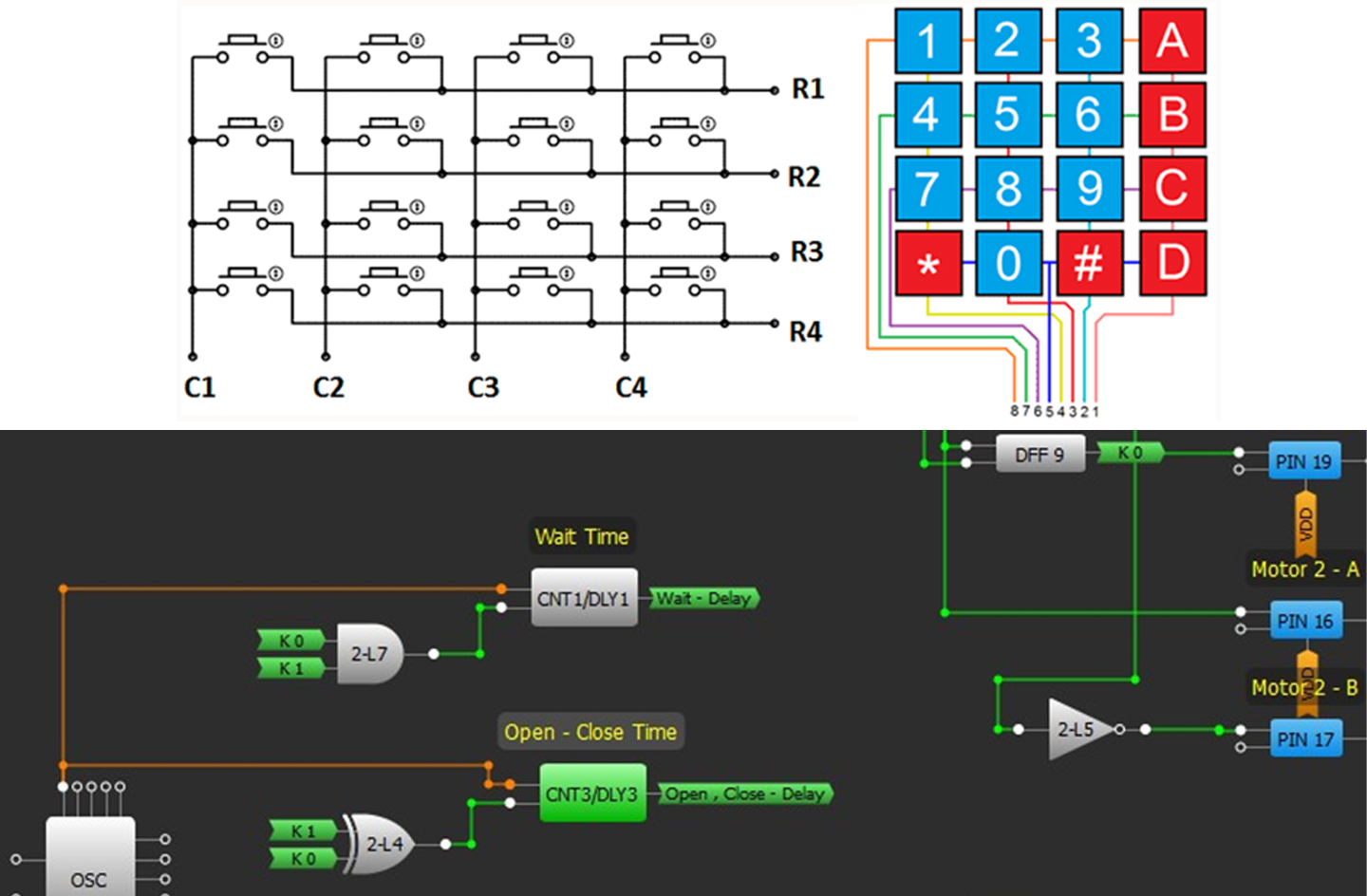
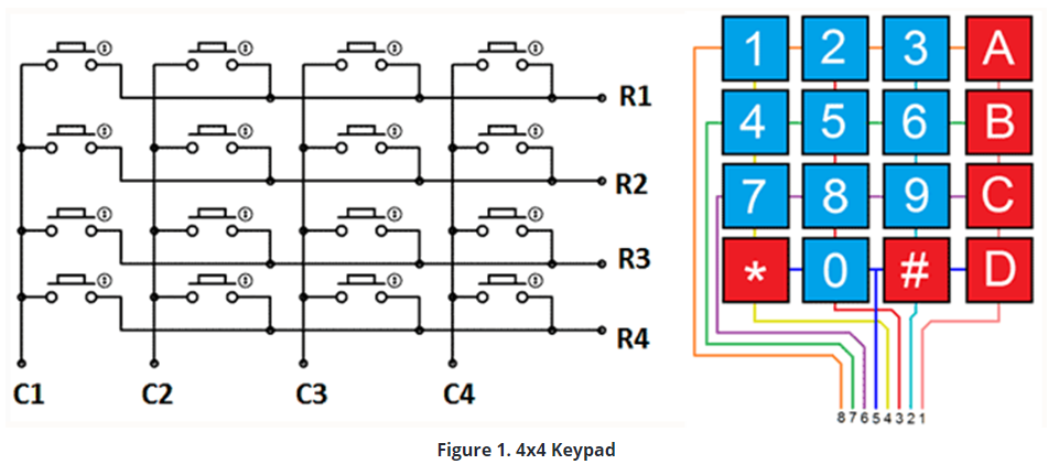
The keypad used in this design is a 4x4 keypad having 4 lines and 4 columns with keys bearing digits, symbols and alphabetical letters. The buttons that users press closes different switches. We sense the button presses by checking the state of these switches.
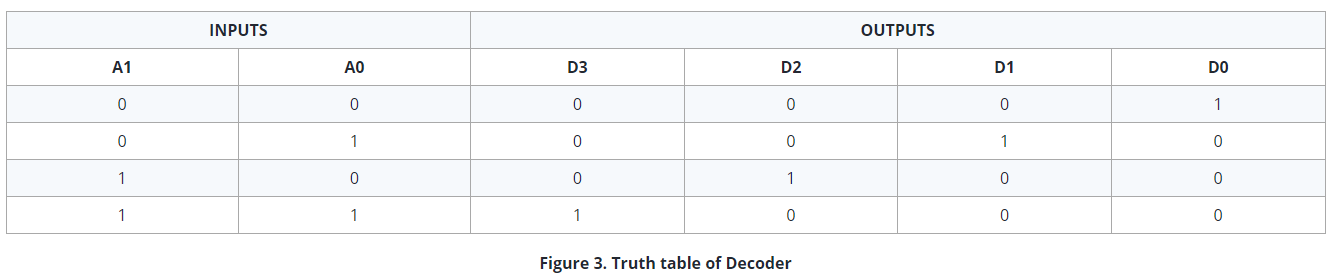
To start the scan process, we apply a logic “1” to each of the lines in sequence, and check the signals that are coming from columns to understand which one is the switch that the user has closed. To give logic “1” to the lines respectively, we used a decoder. The decoder is a circuit that has only one output active dependent on its input states.
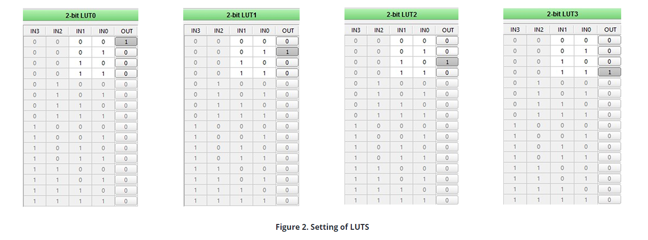
Because only one output is active , a logic “1” can’t be applied to more than one line at the same time. That makes the data that it is receiving true. The decoder was designed as 2x4 because the keypad has 4 lines. We can make a 2x4 decoder using four 2 bit LUTs. Settings of LUT’s and truth table of the decoder are shown in Figure 2:
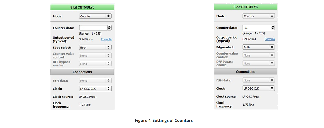
Input of the decoder was set using two counters. In that way, the lines are scanned continuously. As seen in the decoder truth table, the changing time of Input 1 is 2 times longer than Input 0. That’s why the output period of CNT6 counter is set to be 2 times greater than output period of CNT5 counter.
The counter settings are shown in Figure 4.
In the settings, ‘LF OSC CLK’ was selected as CLOCK. This results in a larger output period because the frequency of LF OSC CLK is low. OSC/LF OSC power mode is needed to be selected as Force Power On to use LF OSC CLK.
The counter outputs connect to the clocks of DFFs, and in this way the decoders inputs won’t change during the time of period. The important point here is doing logic AND operation with the inverse of the signal that comes from columns before connecting outputs of counters to the clocks of DFFs. This will ensure that the active line remains stable when a button is pressed.
The scanning function is stopped when a button press is detected, which further ensures the validity of the resulting data.
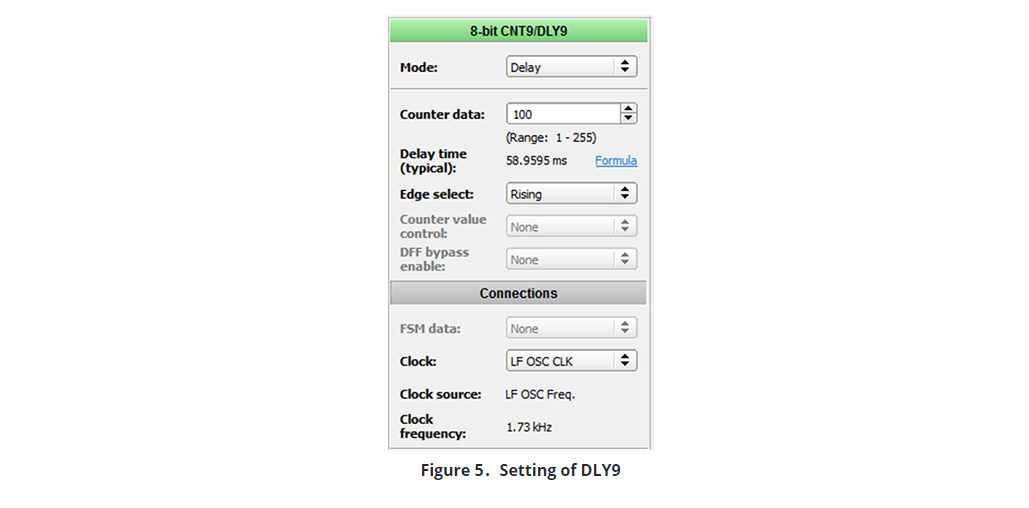
Pushbuttons often create multiple open/close transitions when pressed, due to mechanical and physical behavior. These transitions may be read as multiple presses in a very short time. To prevent this, a timer is used to check twice in a short period of time to make sure the pushbutton is definitely pressed. To accomplish this we create a de-bounce function by adding delay to the signals that come from columns, and perform a logic AND operation to this signal with original signal. We have set up CNT9 / DLY9 as mode delay, with the configuration setting shown in Figure 5.
Each button press will generate the signal that is used as the CLK for the detect circuitry of the security code. The numbers that we have chosen in this project are in order of 1-5-9. To understand the signals that come from columns associated with these numbers, signals that come from the related line and column multiply. So:
- 1st line for number 1
- 2nd column and 2nd line for number 5
- 3rd column and 3rd line for number 9 is multiplied.
2. Password Control Unit
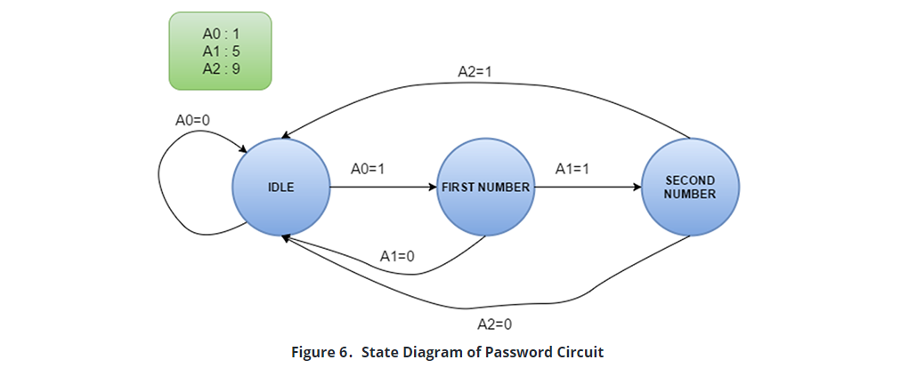
We have checked out the signals that were entered by the user in the previous section. In this section we designed a circuit which compares with required security password with the button press data that is entered. Button data that is input must be entered in correct order to match the 3 digit security password. A circuit that can implement this function can be designed with using the Finite State Machine macrocell.
A state machine is a concept used in designing computer programs or digital logic. The former is comprised of a finite number of states, transitions and actions that can be modeled with flow graphs, where the path of logic can be detected when condisitions are met.
Three different states were used for this circuit. When any button press data is not entered or entered false, the state will become ‘Idle State’. After the first button press is entered with the correct value, the state machine switches to the ‘First Number State’. If a number that is entered is not the correct second number, the state machine switches itself to the ‘Idle State’ again. If the number that is entered is correct, it switches to ‘Second Number State’. If the number that is entered is incorrect while state machine is in second number state, the state machine will switch back to ‘Idle State’ again. If the correct number is entered, the output of the password control unit will be 1. To design this state machine, a state diagram is drawn as shown in Figure 6:
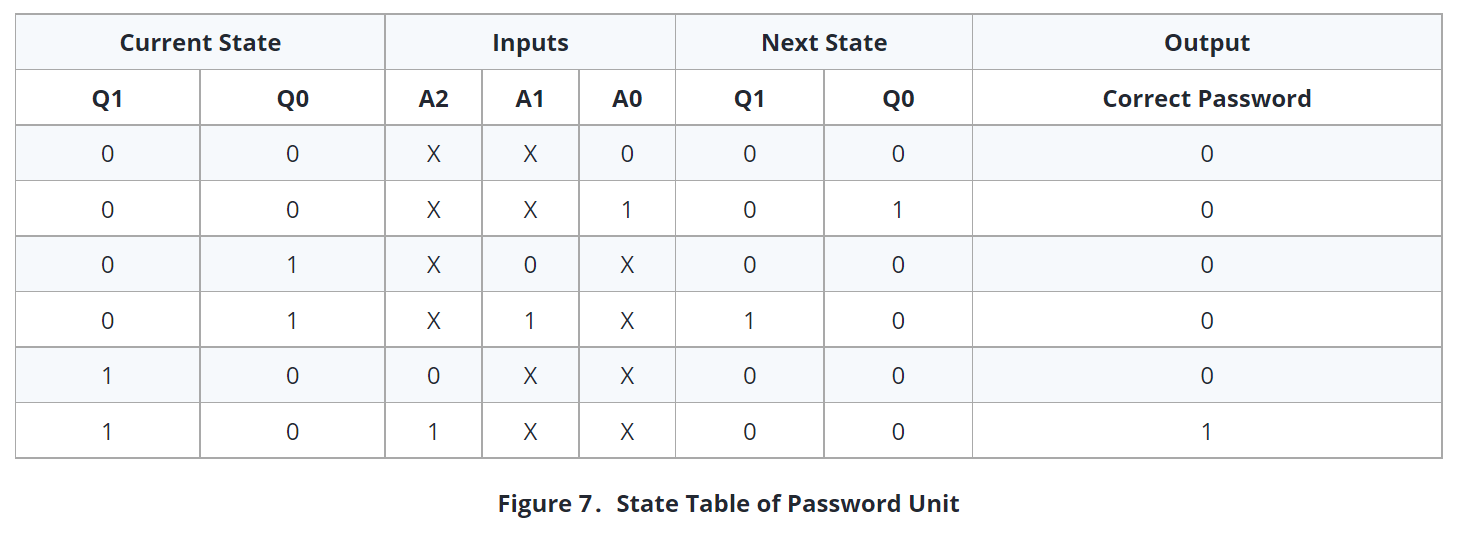
We used 2 DFF’s in our design because the state machine that we have used has 3 states. 2 DFF’s can be used in 4 different states. Then by using this diagram, we created a state table as shown in Figure 7.
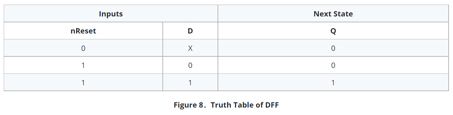
While creating the state table, inputs and present states are written first. According to the inputs that were given to present states, then corresponding next states are written. In next state, inputs of the DFFs are written according to present state and next state. Truth table of DFF is as it is shown in Figure 8.
If a 1 is given to the inputs of DFF, the result will be 1. If 0 is given, it will be 0. The change occurs at the rising edge of CLK and the output of the DFF remains constant until the next logic change is clocked through.
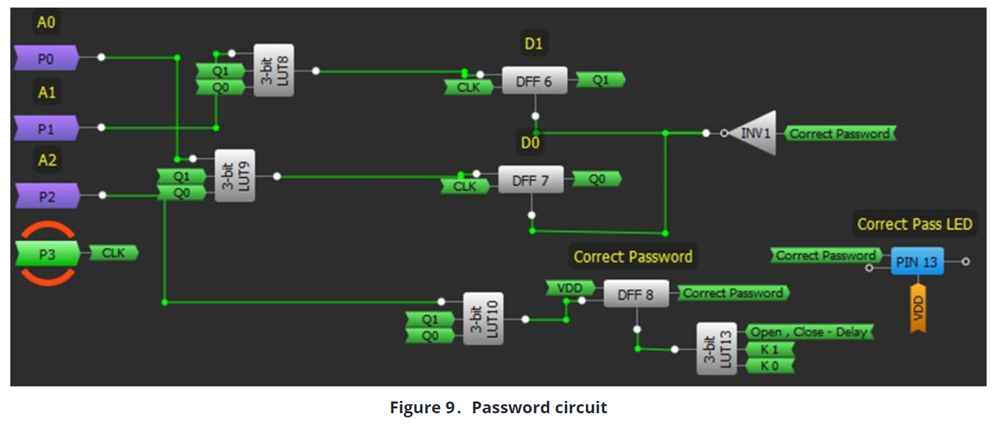
After forming state table, we have found input equations of DFF of D1 and D0 with the aid of this table and truth table of DFF. These equations are as shown below:
D1 = A1 Q1’ Q0
D0 = A0 Q1’ Q0’
Correct Password = A2 Q1 Q0’
After connecting the inputs of the DFFs and its clocks, the circuit will be as shown in Figure 9.
An important point to note here is that the password control circuit will remain in stand-by mode during the period of opening – closing time of the lock. We can make this by inverting the signal of the Correct Password with connecting to the nReset pin of the DFFs. When nReset pin of DFFs are 1, the DFF macrocell works in normal mode, if it is 0, the DFF macrocell is set to reset mode and its output will be 0. When the password is entered correctly, as Correct Password Signal is 1 sets the password control circuit to stand-by mode. We connected the correct password signal to the clock of a DFF and we connected VDD signal to the input of this DFF to keep the correct password signal as 1 during the opening – closing time of the security lock. In this manner, when the correct password signal is active, DFF output will be 1.
Finally, after opening – closing process is finished, Lock State Signal has been sent to nReset pin of this DFF to start a new cycle of the security code comparison.
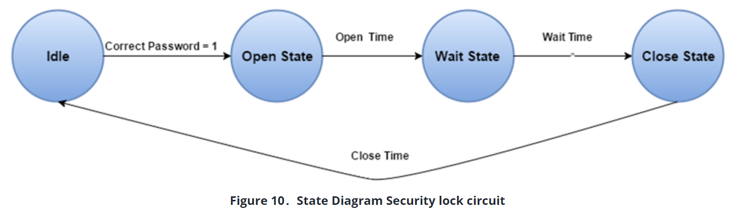
3. Security Lock Circuit
The Security lock circuit is the last stage that becomes active (with correct password signal coming from security password circuit) and controls the drivers that will actuate the security lock. There are 4 different stages in this circuit. These are:
- Idle State – this is the initial state before security lock circuit becomes active.
- Opening State – Allows the opening of the lock by enabling the drivers
- Waiting State – Stops the drivers, and keeps the lock open for a set period.
- Closing State – Allows the closing of the lock by reversing drivers
The state diagram of the security door unit is as it’s shown in Figure 10.
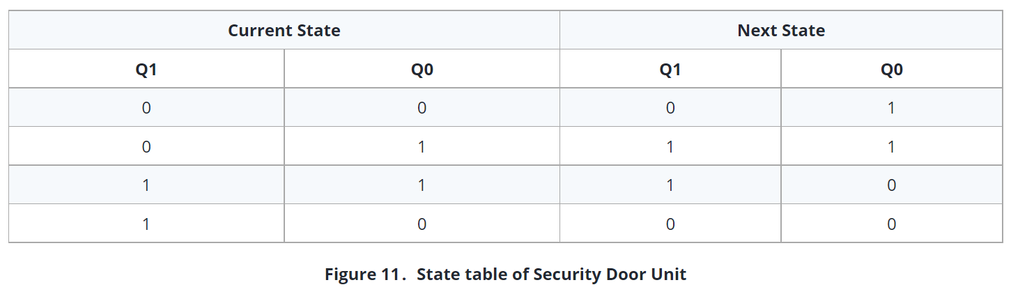
Unlike the previous diagram, changes of the state in this diagram occurs depending on timed period, not depending on inputs. Also, states move in a certain order. The state table for the Security Door Unit is as follows:
According to this table, we can write following equations for the inputs of DFFs.
Door State DFF – 1 = K0
Door State DFF – 0 = K1’
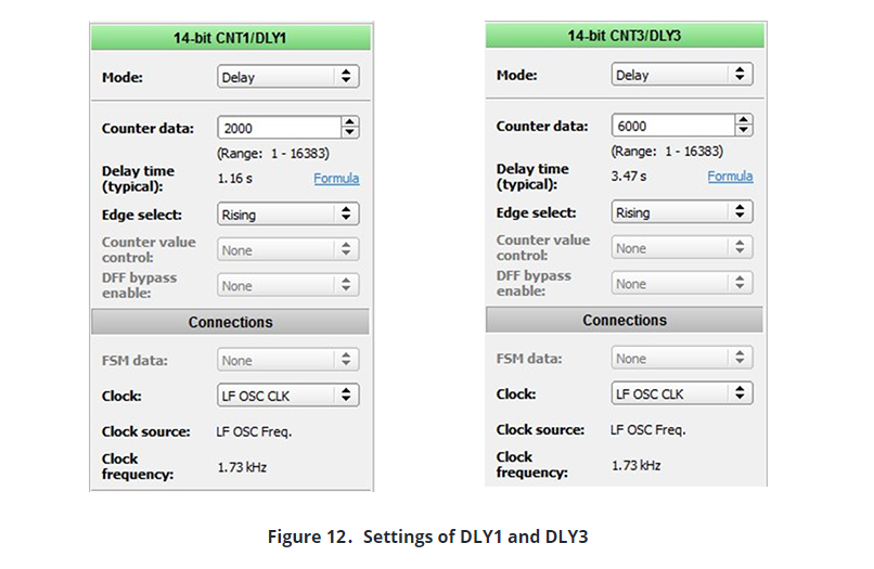
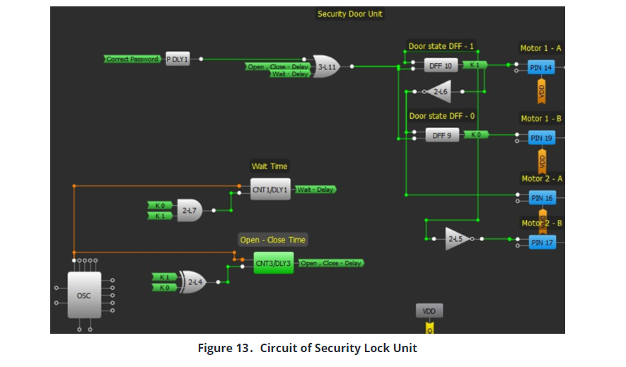
We used DLY1 and DLY3 to set opening-waiting-closing time of the security lock. The settings for these units are shown in Figure 12:
An important point here is the connection of the DFF output corresponding to the opening-closing and standby state to the DLY IN pins of the DLY circuit. We connected K0 and K1 signals to the DLY IN pin of DLY1 which we have set for standby state by using logic AND process. In this way, when state machine passes to ‘K1K0=11’ state, DLY IN pin will be 1 and at the end of the delay time, output of the DLY1 will be 1, and sends a signal to the state machine to pass to the next state. After state machine passes to next state, DLY1 is reset because input of DLY1 is going to be 0.
The same situation is also available for opening-closing state. Because opening-closing time will be same, using only 1 DLY circuit is enough. We connected K1 and K0 signals that come from state machine to DLY3 unit by doing logic XOR process for which we have used DLY IN pin of DLY3 unit to arrange the opening-closing time to be active in the opening-closing states. When the state machine is either K1K0=01(open) or K1K0=10(closed), the DLY3 is activated and at the end of the specified period, the output of DLY3 unit is activated and sends a signal to state machine to pass to the next state. These signals are connected to CLK pins of the state machine by doing logic OR operation. The first signal which will actuate the state machine is the correct password signal coming from control circuit of security password. But before connecting this signal to the clock of the state machine, we should connect to PDLY block. After setting the mode of PDLY block as ‘Rising Edge Detector’ we can connect PDLY output to the clock of state machine by doing logic OR operation with the signals that come from other DLY blocks.
If we do not use PDLY block, the result of logic OR operation will be instantly set to 1 because the correct password signal is 1. This situation can be prevented by using PDLY block. When PDLY block catches ‘Rising Edge’, it generates a one-shot pulse. In this way, the result of the LOGIC OR operation will not always be 1, and changes on the other signals can influence the results of the logic OR operation.
A DC motor is used to open and to close the security lock. High current and high voltage is required to run a DC motor, greater than the value that can be provided by the SLG46620V GreenPAK4 device. So a separate drive circuit that runs a DC motor is taken from another device in the system. This driver is controlled with signals coming from SLG46620V. If we send 1 and 0 to one another to the control pins on the motor driver, motor starts rotating. If we would like to change the rotation of the motor, the signals given to the motor driver must be reversed. 0 or 1 is given to both pins to stop the motor. DFFs that are used for states been set in accordance with this logic in this project. 01 in open state, 10 in closed state, 11 in stand-by state, 00 in idle state. Signals that are output from the state machine can be directly connected to the motor driver. These signals can be connected in reverse for a second motor. After all connections are made, a security lock unit is shown in Fig. 13.
Conclusion
In this project, we demonstrated how to complete a design described by a state machine, and implemented it with a single GreenPAK IC. Additionally, consideration is given for driving motors or actuators. Indicators or other functions can be added as well since there are extra circuits still available within this programmable mixed-signal IC.