This project presents a low cost and low power DC/DC push-pull converter based on the GreenPAK SLG46108 device.
Galvanically isolated interfaces are a common requirement within industrial devices for safety reasons. In this type of application, a digital isolator is used to galvanically isolate an MCU from a communication transceiver or an ADC.
Digital isolators work at two power domains, using an isolated DC power supply in one domain. The low DC voltage for isolated power domain could be achieved with a small and simple push-pull converter. The push-pull converter is a transformer-isolated topology using two transistors switching in complementary mode.
This project will present a low cost and low power DC/DC push-pull converter based on the GreenPAK™ SLG46108 device. The following sections will show how to:
- Generate a complementary PWM with dead time using the programmable delay block.
- Generate a start-up sequence using a pipe-delay block.
- Obtain multiple clock frequencies via an internal oscillator.
The complete design file can be found here. It was created in the GreenPAK Designer software (a part of the Go Configure™ Software Hub).
1. Operation Principle of Push-Pull Topology
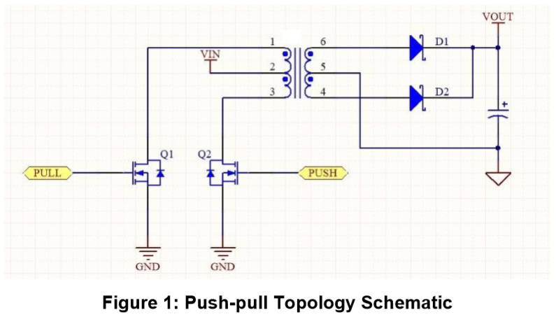
A push-pull converter schematic topology is shown in Figure 1. This converter uses a transformer with center-tap in the primary and secondary windings. Two transistors (Q1 and Q2) work to switch the DC input voltage VIN in alternate half-cycles.
On the primary side, when the PUSH command signal (Figure 1) is HI, Q2 transistor is turned on and transformer current flows from Vin to Q2 transistor. Simultaneously in the second winding a transformer current flows from diode D1 to the output capacitor, returning through the center-tap.
The PUSH command is HI during one half cycle. The PULL command is high during the other half cycle. When the PULL command is high, Q1 transistor is turned on and the current flows from VIN to Q1 in the primary, and from D2 to the output capacitor in the secondary.
The current flows in the same direction in the output capacitor during both current cycles, keeping a positive output voltage VOUT. The converter output voltage could be given by equation (1): VOUT = 2 * D * VP * n - VDIODE
Where VOUT is the output voltage, D is the duty cycle, VP is the voltage in the transformer primary winding, n is the transformer turn-ratio and VDIODE is the voltage drop in outputs at diodes (D1 and D2). Vp is given by equation (2): VP = VIN - VDS, where VDS is the voltage drop from the internal resistance of transistors Q1 and Q2.
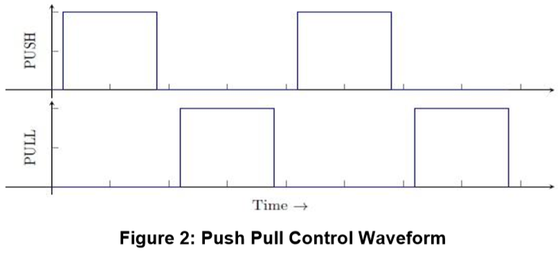
An issue with this topology is the variation on output voltage with load current change. To ensure a stable output voltage a linear regulator should be added to the output, and the converter output voltage must be higher than the minimum specified for the regulator. The PUSH and PULL command signals are shown in Figure 2. Command signals are complementary and should have the same duty cycle to avoid transformer core saturation.
An important aspect for push pull converters is the need for a short time interval where both commands are low, as can be seen in Figure 2. This time interval is required to avoid the short circuit of both primary ends of the transformer.
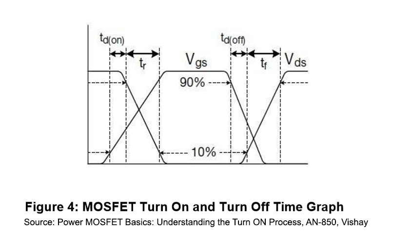
The transistors Q1 and Q2 require a small amount of time to effectively turn-on and turn-off. The MOSFET turn-on and turn-off involves a process of charging and discharging a MOSFET gate. A common approach is to model MOSFET gate charge influence as capacitors between MOSFET source and drain. This is shown in Figure 3.
In datasheets the turn-on and turn-off transitions are presented as shown in Figure 4. However, the switching times are highly affected by circuit conditions, such as gate drive resistance, drain-source voltage, etc.
The time interval is short and should be generated by the driver, which generates a dead time interval between the switches command. The push pull duty cycle is lower than 50 % because of dead time interval. That usually reduces duty-cycle by 3-5 %. This reduction in duty cycle lowers the output voltage and increases dissipation losses.
2. Board Schematic and Layout
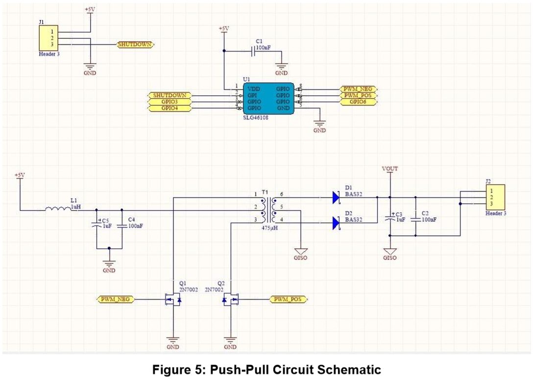
Figure 5 depicts the board schematic of a low power converter module using the SLG46108. The module has an input DC voltage of 5 Volts (J1 connector) and an isolated output with more than 5 Volts. Output voltage (J2 connector) is higher than 5 V to enable the operation of a linear regulator.
In this circuit the SLG46108 generates the control signals PWMPOS and PWMNEG to switch the two transistors Q1 and Q2. The PWM signal is active when SHUTDOWN input is low or is left open. When SHUTDOWN is high the PWM signal is inactive and both transistors are turned off.
The switching dead time interval is defined to generate a duty cycle of 45 %, considering a switching frequency of 250 kHz. This approach enables the use of different transistors with the developed controller. The drawback is the reduction in the output voltage and the reduction in efficiency.
The selected transformer is the Wurth Electronic part-number 760390014 that has a turns-ratio of 1:1.3. The output diodes are the part-number BAS32, from Nexperia. For this project we have considered the maximum diode drop-out voltage as 0.7 V. Both transistors are the well-known 2N7002 NMOS.
For this circuit we calculate the expected minimum output voltage, when the diode drop-out voltage is maximum, using equation 1. Then:
VOUT = 2 * 0.45 * 5 * 1.3 − 0.7 = 5.85 − 0.7 = 5.15 V
The drop-out voltage in transistors is neglected for simplicity, as the load current is low and the MOSFET equivalent resistance is low too. The output voltage must be higher than the calculated minimum voltage, especially at light loads.
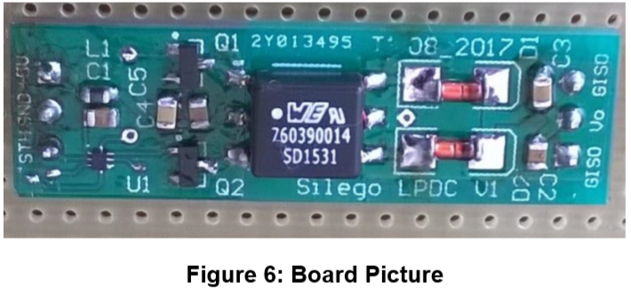
Figure 6 shows a picture of the mounted module board:
3. SLG46108 Schematic
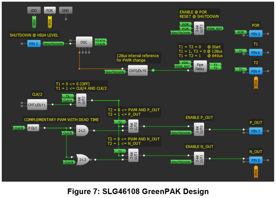
The project design developed in GreenPAK Designer is shown in Figure 7.
3.1. Clock Configuration
The implemented solution uses a 250 kHz clock signal (CLK/8) from the OSC block as the base PWM signal. The OSC block is configured to a main clock frequency of 2 MHz (CLK) and two of its outputs are used: the clock divided by four (CLK/4) and by eight (CLK/8). The main oscillator clock is sourced to block CNT1/DLY1 to generate a clock divided by two (CLK/2).
3.2. PWM Configuration
To generate the complementary PWM signal with a dead time between the transitions, we used the structure of block P DLY, 2-L2 and 2-L3. Base PWM signal of 250 kHz frequency is delayed in Programmable Delay block by nearly 222ns (2 cells delay at 5 V). These two signals are inputs to blocks 2-L2 and 2-L3. Block 2-L2 is an AND logic port and the output will be high only when the CLK/8 and his delayed version are high. Block 2-L3 is an NOR logic port and the output will be high only when CLK/8 and his delayed version are both logic low.
This structure generates the complementary PWM signal with the same duty cycle in both outputs and a dead time interval between transitions. Before output signals OUT P and OUT N can drive output pins, the signals should pass through blocks 3bit-LUT0 and 3bit-LUT1.
3.3. Design Start-up
Blocks 3bit-LUT0 and 3bit-LUT1 are part of the design start-up logic. Start- up sequence logic is required in the converter to avoid high inrush current during initialization. The start-up process has two phases that are controlled by the signals T1 and T2, generated via a Pipe Delay block. The Pipe Delay block starts counting pulses of the CNT0/DLY0 block after block reset. The CNT0/DLY0 block generates a pulse every 128 µs. This keeps the T1 and T2 signals LO during the first 128 µs of operation.
3.4. T1 and T2 Signals
T1 signal is an input for 3bit-LUT2 block. The LUT2 block sends a PWM signal with a small duty cycle generated by the AND operation of signals CLK/4 and CLK/2 when T1 is high and a continuous LO signal when T1 is low.
The T2 signal is an input for 3bit-LUT0 and 3bit-LUT1 blocks. The T2 signal is used in these blocks to select the duty cycle of the output PWM drive signals. When T2 is LO the signals OUT P and OUT N are ANDed with the signal PWM that comes from block 3bit-LUT2. In this situation the output signals P, from 3-bit LUT0, and N, from 3-bit LUT1, have the same duty cycle of PWM signal. When T2 is HI the output signals P and N are the same as OUT P and OUT N. If T2 and T1 signal are both low, PWM signal is always low and the outputs P and N will be always low too.
This group of blocks enables the control of PWM output signals using T1 and T2. After the initial 128 µs LO signal both PWM outputs will have a small duty cycle, until T2 signal rises to high level. A T2 signal rise to high logic level will happen after 640 µs of the start operation, or after 512 µs after the rising edge of T1 signal.
3.5. PWM Output Signals
The PWM output signals P and N drive the output pins. They pass through two enable blocks, the 2bit-LUT0 and 2bit-LUT1. These blocks enable output signals when SHUTDOWN signal is low. When SHUTDOWN signal is high the output will be always low. SHUTDOWN signal is an input signal from PIN2.This pin is configured with a pull-down of 1 MΩ and is used to put all the circuit into a low power mode. When SHUTDOWN is high the oscillator is put in low power mode and Pipe Delay block is reset. This procedure guarantees the application of start-up logic after SHUTDOWN signal falling, turning on the circuit again. The block 3bit-LUT3 is used to enable Pipe Delay counting only after the rising of POR signal and when SHUTDOWN signal is low.
PIN 8 and PIN 7 are outputs that receive the PWM signals from 2-bit LUT1 and 2-bit-LUT0 respectively, driving the two transistors Q1 and Q2. PINs 6, 4 and 3 are configured as outputs and receive signals T1, T2 and POR respectively. These signals are used for the measurement of startup signals only.
4. Measurements
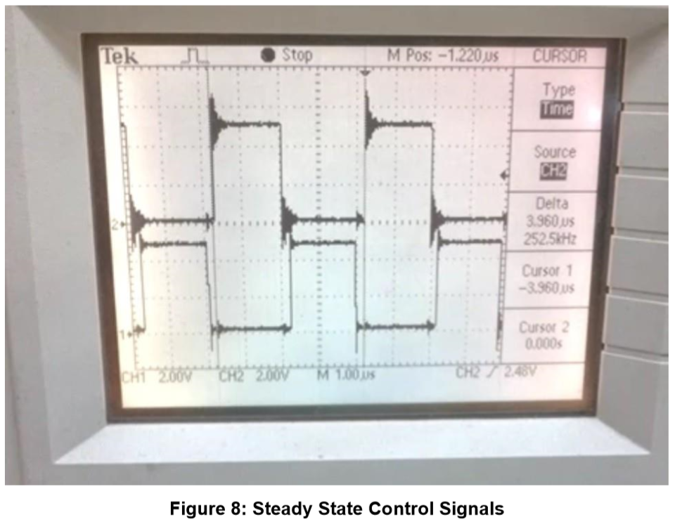
The board module was tested for an input voltage of 5V and the control signals were measured with an oscilloscope.
Figure 8 shows the complementary output PWM when the circuit is in steady state operation. The measured PWM frequency is 252.5 kHz, near to the expected 250 kHz frequency.
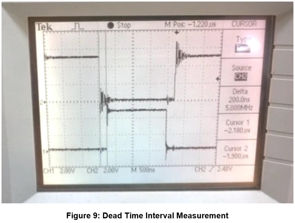
Figure 9 shows the measurement of the circuit dead time interval. The difference between cursor 1 and 2 is about 200 ns, nearly the expected value of 222 ns.
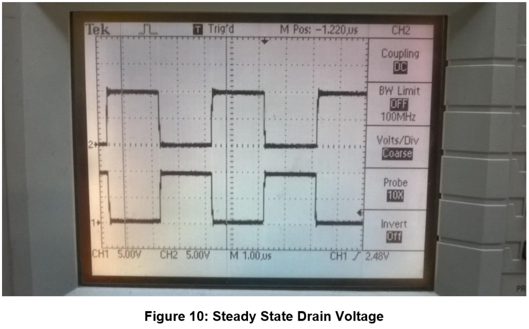
The voltage on the drain of Q1 and Q2 MOSFET is shown in Figure 10. The voltage is low when the MOSFET is conducting. The voltage in the drain MOSFET is double of VIN when it is off, because of the voltage reflection on the primary.
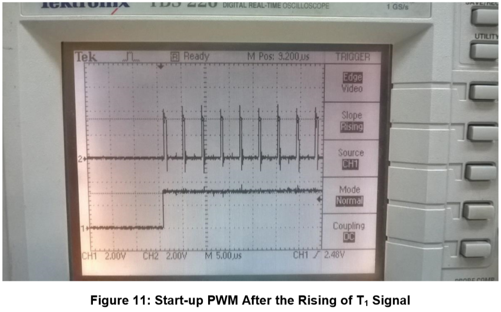
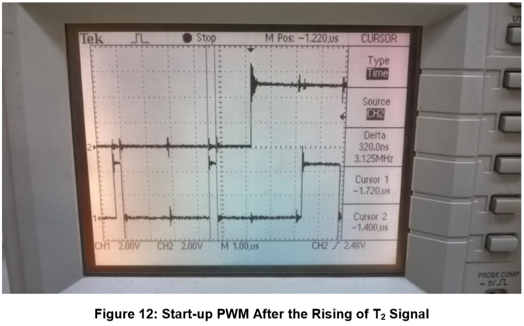
During start-up the control generates a PWM that has a reduced duty cycle. It can be seen in Figure 11. Figure 12 shows the duty cycle change after the rising edge of T2 signal. The transistor On time is measured as 320 ns during the first PWM cycle.
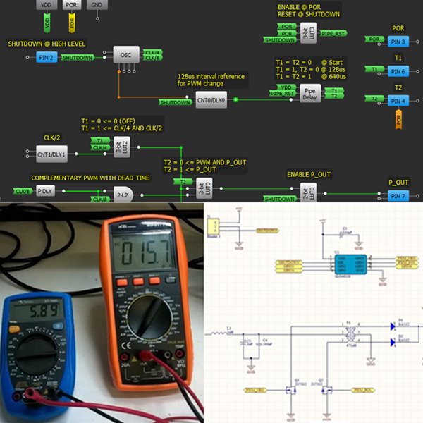
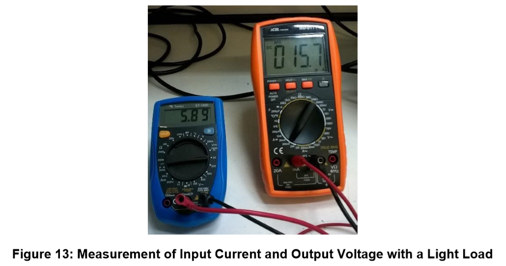
Converter output voltage and input current were measured with a 10 KΩ resistor in parallel with a 1 KΩ resistor. The measured voltage is 5.89 Volts and input current was 15.7 mA, as shown in Figure 13.
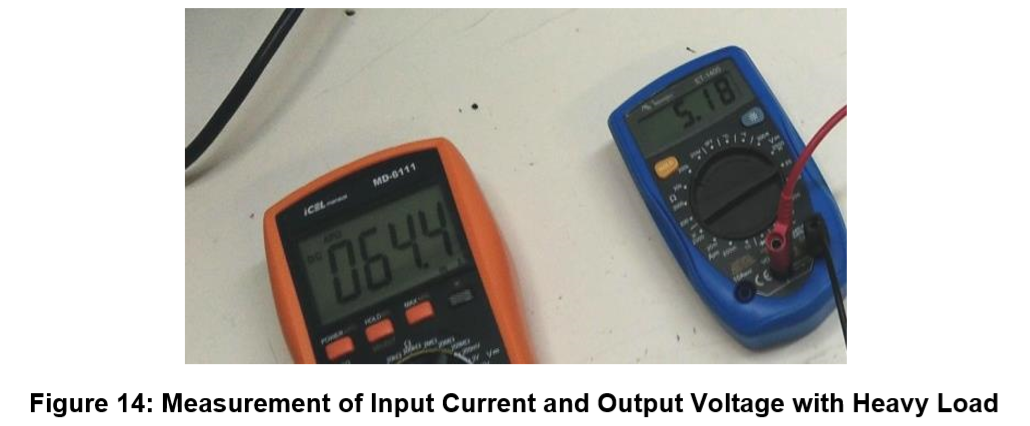
The output voltage and input current were measured with a heavy load of 120 Ω resistor too. The measured voltage is 5.18 Volts (almost 44 mA output current) and input current was 64.4 mA, as shown in Figure 14.
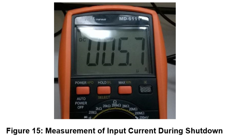
The circuit input current during shutdown was measured too, achieving 5.7 µA of current, as can be seen in Figure 15. The most significant part of shutdown current is from the presence of 1 MΩ pull-down resistor.
Conclusion
This project presented how to implement a low power and small-factor DC/DC push-pull converter with a GreenPAK IC. The main advantage of GreenPAK over other solutions is the presence of a programmable delay block. This block makes the design of dead time insertion logic really simple. It is interesting to see how it was possible to add a personalized start-up sequence using pipe delay block and the addiction of a shutdown mode control. Although this circuit was designed to operate on supply voltage of 5 Volts, it can also work at a supply voltage of 3 Volts. The only limitation on the supply voltage is the threshold voltage of MOSFETs and maximum IC supply voltage.