This project describes a simple hardware implementation of a 4-Mux LCD driver using time-division multiplexing technique
Below we described steps needed to understand how the solution has been programmed to create the system monitor 4-MUX LCD driver. However, if you just want to get the result of programming, download GreenPAK™ Designer software to view the already completed GreenPAK Design file. Plug the GreenPAK Development Kit into your computer and hit the program to design the device.
Liquid crystals are commonly used to create simple screens for electronic systems like digital clocks and car audio faceplates.
In an LCD, the liquid-crystal controls whether the segments appear ON or OFF by interacting with the light traveling through the LCD. When a voltage is placed across a segment, the internal molecules align with the electrical field across it and allow light to pass through unobstructed. When no voltage has been placed across the screen, the light travels through the liquid crystal and rotates 90˚. In both cases, the light travels through the front and rear polarized filters that block / pass the light depending on its polarization.
LCDs are unique such that their light sources can be either passive or active. For passive displays, external lights are used to illuminate and view the characters on the display. Active displays, on the other hand, are designed with an internal light source on the back of the screen.
For a detailed description of how LCDs work, please refer to [8]. This article breaks down both the physical components and the scientific theory behind LCDs. It also describes the benefits and drawbacks of various LCD types including reflective, transmissive, and transflective displays.
This project improves upon the design described in [8] by offloading many of the processing and hardware requirements from the MCU onto a small and inexpensive GreenPAK IC.
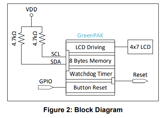
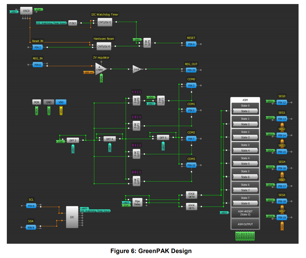
Figure 2 shows the block diagram of this proposed solution. In addition to the LCD driving circuitry, the GreenPAK solution includes system monitoring features like hardware resets, watchdog timers, and RAM storage.
1. Creating Drive Signals for LCD Screens
LCDs are deceptively similar to LED screens in that they both require a DC voltage to turn on their segments, but the similarities end here. In fact, placing a sustained DC voltage across an LCD segment will damage the liquid crystal. The following sections detail a few techniques used by designers to maintain an average of zero volts across the individual LCD segments.
1.1. LCD Driving Techniques: Static Drive and Multiplex Drive
When designing drive circuitry for a small LCD like a 7-segment display, there are generally two different categories: Static Drive and Multiplex Drive.
1.1.1. Static Drive Technique
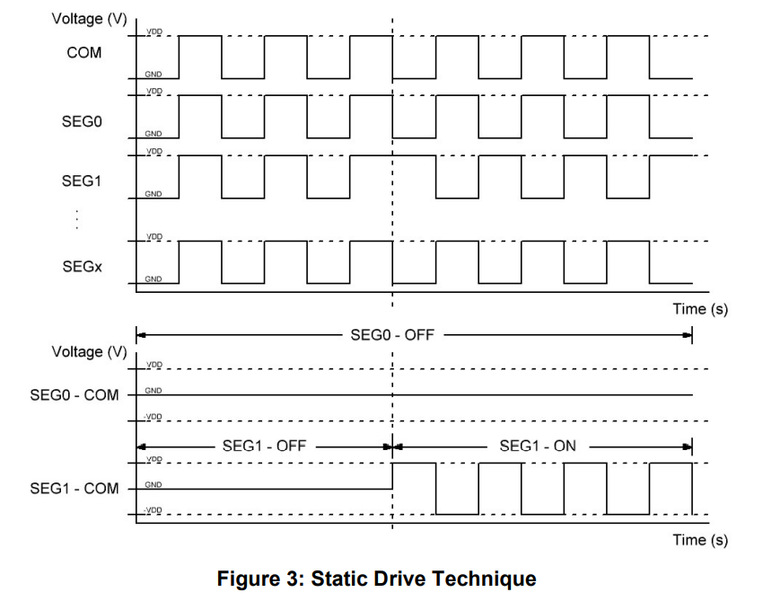
Static Drive LCD segments have two connections: a single common line shared amongst each of the segments and a unique control signal for each segment. To avoid creating a non-zero DC average voltage across a segment, the COM line and the SEGx lines are driven with square waves as shown in Figure 3. The difference between the SEGx lines and the COM line generates a DC voltage across each of the segments without changing the average DC voltage across the segment. To enable the LCD segment, simply invert the square wave driving the specific segment of interest. The average voltage across the LCD segment will still be 0 V.
The Static Drive technique is simple and quick for small LCDs. It doesn’t require special voltage levels or complicated timing behavior, but the GPIO requirements impact the viability of this technique for high-segment-count displays.
1.1.2. Multiplex Drive Technique
The Multiplex Drive technique reduces the GPIO requirements for driving larger LCDs. The basics of this technique center around using multiple COM lines for specific SEG lines. Using time-domain multiplexing, each segment can be individually enabled on one COM line.
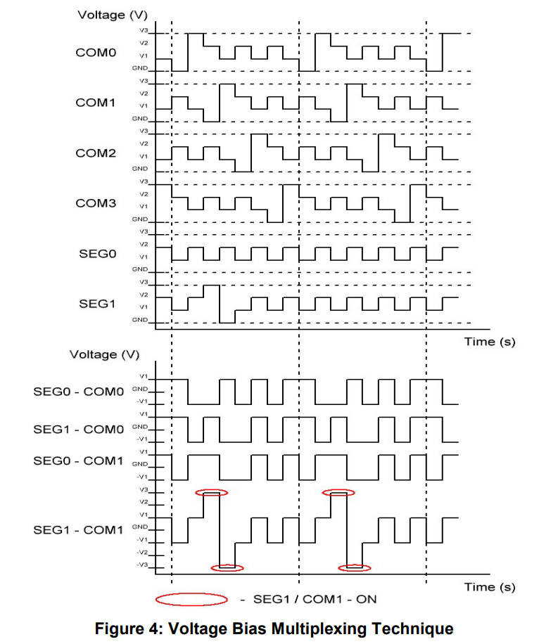
Figure 4 shows the first Multiplex Drive technique which uses multiple voltage bias levels to drive each of the SEG and COM lines. Whenever the voltage difference between SEG and COM exceeds V1, that particular SEG/COM pair turns on.
This technique is based on time-division multiplexing of the COM lines. Each of the 4 COM lines is sequentially activated to interact with the SEG lines. During the active period of a COM line, the SEG lines can be inverted and driven to the opposite rails to enable the SEG/COM pair.
When averaging the difference between the SEG and COM lines over one period, the average DC voltage remains at 0 volts. A significant drawback to this technique is that it requires an analog GPO with the capability of producing 4 different output voltage levels.
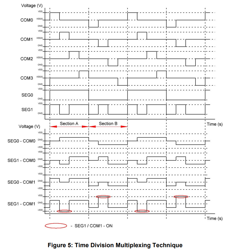
The second technique, shown in Figure 5, operates off the same time-domain multiplexing principles described in the voltage bias multiplexing architecture. To reduce the number of required output voltage levels, this technique doubles the period to maintain an average of 0V across the LCD segments. Figure 5 shows that SEGx signals in Section B are inverse signals of Section A. Whenever the difference between SEG and COM equals VDD or -VDD, that SEG / COM pair turns on. This technique assumes the magnitude of the segment’s turn-on voltage is between VDD/2 and VDD.
This technique takes advantage of the GPIO input structures to generate the VDD/2 voltage level. By connecting the GPIO to a voltage divider from VDD to GND, the GPIO is used to switch between a highimpedance input and a push-pull output to generate the three voltage levels. This technique uses a standard GPIO to drive each of the COM lines.
The GreenPAK design in this project is based on the second Multiplex Drive technique shown in Figure 5.
2. GreenPAK Design
Figure 6 shows the GreenPAK design which implements the LCD driving architecture along with a 2 V regulator, a watchdog timer, a hardware reset, and 8 bytes of RAM into one design. The 2 V regulator accommodates the 1.7 V to 2.2 V operating voltage range of the LCD.
2.1. COM Signal Generation
The COM signals are generated, as previously described, by modifying the GPIO settings and using an external resistive divider set at VDD/2. The GPIO control signals originate from the oscillator-driven DFF chain as shown in Figure 6. These signals determine whether the GPIO is configured as an input or an output and whether the GPIO is HIGH or LOW.
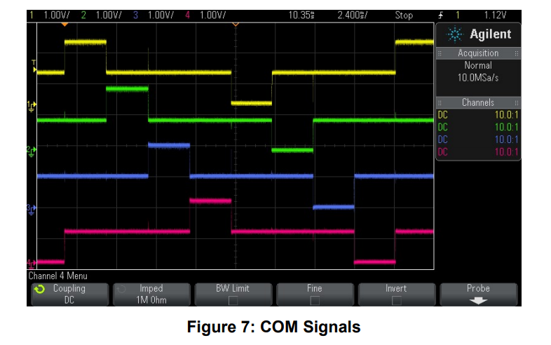
As one can see, the COM signals shown in Figure 7 match the COM signals shown in Figure 5.
Note: VDD = 2.0 V, external divider bias set at VDD/2 for High-Z mode
Channel 1 (Yellow) – COM0 (PIN3)
Channel 2 (Green) – COM1 (PIN5)
Channel 3 (Blue) – COM2 (PIN7)
Channel 4 (Magenta) – COM3 (PIN10)
2.2. Segment Signal Generation
ASM Configuration
In this design, the ASM is re-purposed as a fancy pattern generator to drive the SEG outputs. In Figure 6, the Pipe Delay block is used to cycle through the various ASM states.
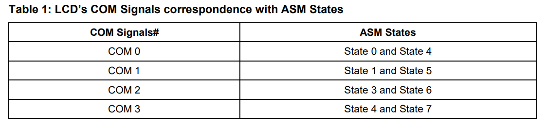
The GreenPAK ASM consists of 8-states where each LCD COM line corresponds to two ASM states. Table 1 lists the ASM states with their associated COM lines.
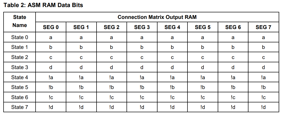
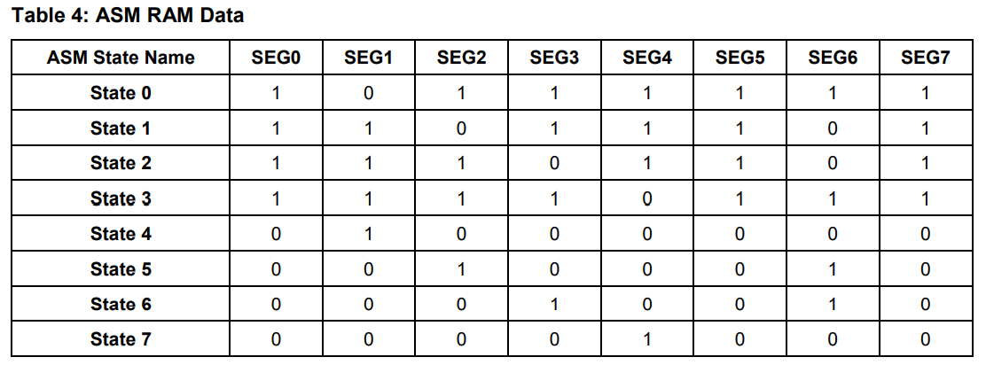
Each ASM state holds a byte of data in RAM to output to the connection matrix. Table 2 provides a template on how to configure the binary data for each ASM state. Assuming bit a is written to State 0, bit b to State 1, bit c to State 2, and bit d to State 3, the bits in State 4 through State 7 should be inverted to !a, !b, !c, and !d respectively. For example, to turn ON SEG 0 associated with COM 0, write a 0 in the State 0/SEG 0 location and 1 in the State 4/SEG 0 location. This phenomenon of data inversion correlates with the description in the Multiplex Drive Technique section.
Note: VDD = 2.0 V, external divider bias set at VDD/2 for High-Z mode
Channel 1 (Yellow) – COM0 (PIN3)
Channel 2 (Green) – COM1 (PIN5)
D0 – SEG0 (PIN12)
D1 – SEG1 (PIN13)
D2 – SEG2 (PIN14)
D3 – SEG3 (PIN15)
D4 – SEG4 (PIN16)
D5 – SEG5 (PIN17)
D6 – SEG6 (PIN18)
D7 – SEG7 (PIN19)
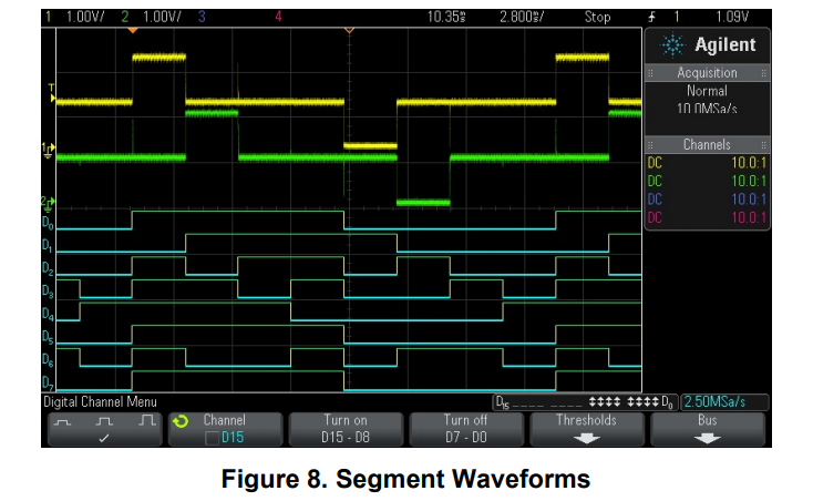
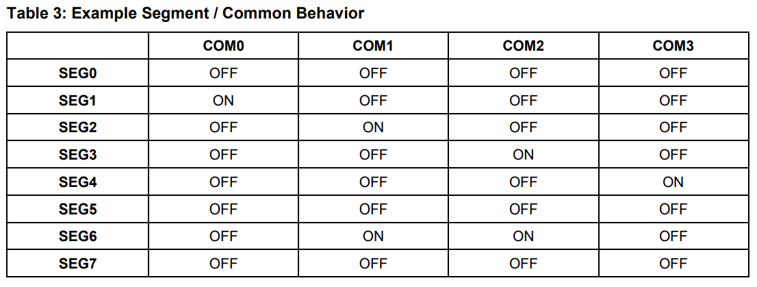
An example of SEG/COM behavior is shown in Figure 8. These waveforms show particular COM/SEG pairs enabled in accordance with Table 3. To enable these COM/SEG pairs, the ASM RAM must be configured to the values shown in Table 4 where a “0” in States 0 to 3 and a “1” in States 4 to 7 represents an ON segment. By analyzing Figure 8 one can decipher the state of the LCD segments by subtracting the SEG signals from the COM signals.
2.3. 2 V Voltage Regulator
Since the operating voltage range for the LCD is 1.7 V to 2.2 V, an internal 2 V regulator limits the GreenPAK’s VDD and determines the logic levels of the COM and SEG signals. This narrow range depends on the specific LCD used in the system. This voltage range, the drive strength of the GreenPAK GPIOs, and the size of the external passive components all impact the contrast of the LCD.
The GreenPAK design uses an ACMP to regulate a 3.3 V supply down to 2.0 V using a resistive divider with a low side NMOS switch. Passive components limit the current flow and determine the transient behavior of this regulator. ACMP0 shown in Figure 6 regulates the voltage to 2 V. Please reference Figure 9 and Figure 12 for a system-level implementation of this regulator.
2.4. Additional Features
To synchronize the SEG and COM signals, the I2C virtual input “nRST” will actively reset the design when asserted LOW. When released HIGH, the SEG and COM signals will be synchronized with each other in the time domain as they both operate from the same 25kHz oscillator. For more information on resetting the ASM with I2C, please reference [6].
System monitoring features such as a hardware button reset, a watchdog timer, and RAM storage are also implemented on the GreenPAK solution. The button reset is controlled externally with the help of a GPIO while the watchdog timer and RAM storage are controlled with I2C communication from the MCU.
2.5. Modifying the LCD Display
Enabling and disabling different segments on the LCD is as simple as rewriting the RAM registers within the GreenPAK’s ASM. To execute the change properly, we recommend the procedure described below:
1. Assert nRST LOW using the I2C virtual inputs
2. Program the new RAM contents into the ASM
3. Set nRST HIGH to initiate the LCD driving signals
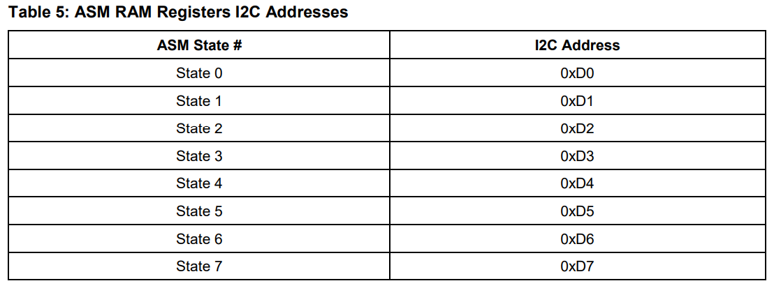
Following the sequence above will guarantee that the COM and SEG pins remain synchronized in the time domain. Table 5 shows the I2C addresses of the ASM states. Data on the LCD is modified by re-writing these ASM RAM registers using I2C.
3. Testing
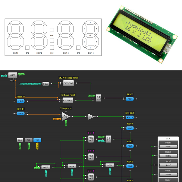
A twisted nematic (TN) reflective LCD display (Mouser #: 696-LCD-S401M16KR) is tested using an Arduino Uno. This LCD display is a 4-digit, 7-segment multiplexed display.
3.1. LCD Pattern Display
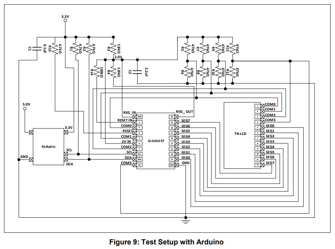
Figure 9 shows the test schematic used to display different patterns on the multiplexed LCD. The I2C lines (SCL and SDA) are connected to the Arduino’s 3.3V output through the R1 and R2 pull-up resistors. Resistors R3 and R4 along with capacitor C2 form the 2V regulator as described in 2.3. R5 through R12 are used to generate bias voltages for the COM signals.
As previously discussed, the LCD contrast depends on both the amplitude and the transient behavior of the LCD drive signals. The sizing of R5 to R12 and the drive strength of the GreenPAK GPIOs impact the transient behavior of the LCD drive signals. Optimal resistance values were determined by iterative bench testing. This external resistor divider network impacts the quiescent current, PCB space, and cost of the system solution. For more information on resistor selection, please refer to [9] and [11].
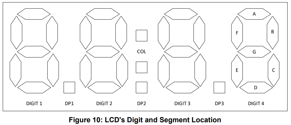
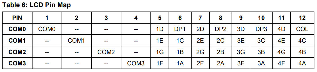
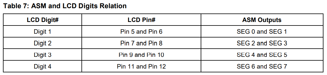
Different patterns are displayed on the multiplexed LCD by following the steps described in 2.5. The LCD’s pin mapping and digit and segment locations are shown in Table 6 and Figure 10 respectively. By correlating Table 6 and Figure 10, it can be determined that pin 5 and pin 6 correspond to Digit 1 of the LCD, pin 7 and pin 8 correspond to Digit 2, pin 9 and pin 10 correspond to Digit 3, and pin 11 and pin 12 correspond to Digit 4. This correlation is shown in Table 7 along with the corresponding ASM outputs.
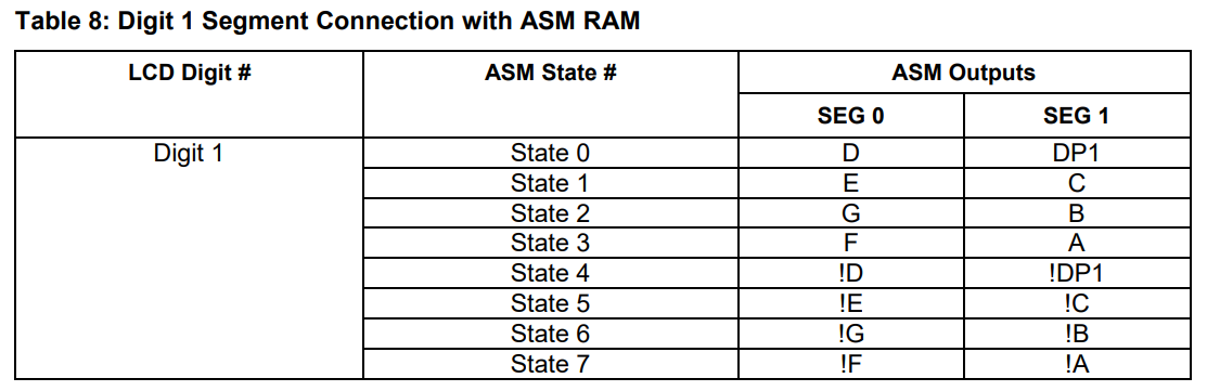
The SEG 0 and SEG 1 outputs of the ASM control Digit 1 of the LCD. Similarly, SEG 2/3, SEG4/5, and SEG6/7 control Digit 2, 3, and 4 respectively. Table 8 shows the Digit 1 and ASM output connections. Table 1 and Table 8 show that one must write a “0” to State 0/SEG 0 and a “1” to State 4/SEG0 to turn ON segment D on Digit 1. Similarly, other segments can be enabled/disabled by writing respective State x/SEG y locations.
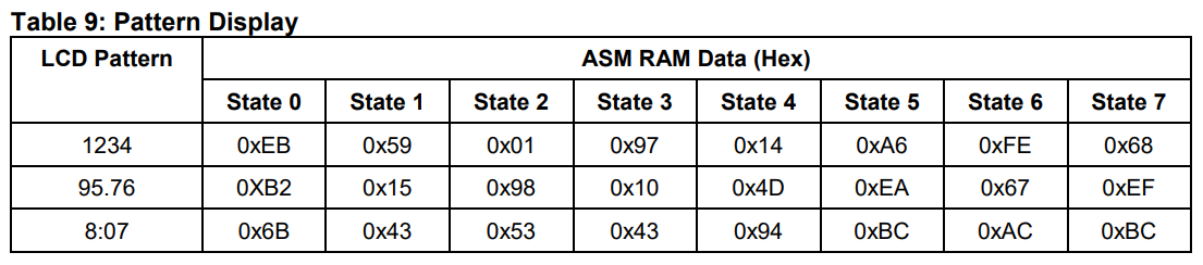
To display a pattern on the LCD, the binary data is first converted into the hexadecimal format and then written to the ASM RAM registers. To display “1234” on the LCD, for example, follow the I2C procedure listed in 2.5. The I2C commands for writing data into the ASM RAM registers are as follows:
[Start 0x08 0xF4 0x00 Stop]
[Start 0x08 0xD0 0xEB 0x71 0x01 0x97 0x14 0x8E 0xFE 0x68 Stop]
[Start 0x08 0xF4 0x01 Stop]
Here, 0x08 is the I2C slave address and 0xF4 is the word address for the I2C virtual inputs. There are various I2C slave addresses available in the GreenPAK. For more information on I2C communication please visit [5].
Table 9 shows a few example patterns and the respective hexadecimal bytes required by the ASM RAM.
Some example code for controlling the LCD using an Arduino Uno is included in this ZIP file.
3.2. LCD Reliability
The LCD reliability is dependent on the average DC offset voltage of the LCD drive signals. The DC offset is measured as the difference between the amplitudes of the COM and SEG signals over time. If the average difference is on the order of 50mV or greater, the DC offset will eventually damage the LCD. For more information on acceptable DC offset specifications, please refer to [12].
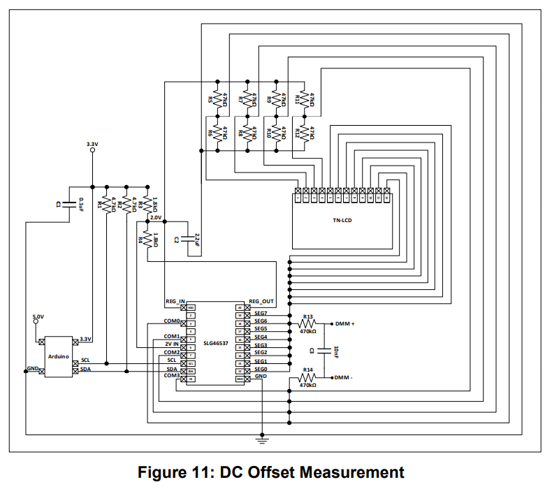
Figure 11 displays the test setup used to measure the presence of DC offset in this solution. R13, R14, and C3 create a high impedance measurement interface to monitor the average voltage using a digital multimeter. The resistors chosen for the DC offset measurement are approximately ten times greater than the resistors used in the design to avoid loading the resistive divider network.
The DC offset was measured at about 5mV. As this offset is less than the 50mV offset criteria, the LCD should not be damaged
4. Design Considerations and Solutions
There are certain criteria that should be considered when evaluating this design. These criteria include the operating voltage range of the LCD, the drive strength of the GreenPAK GPIOs, external component selection, and low power optimization.
The operating voltage range for the tested LCD ranges from 1.7V to 2.2V. When operating outside this range, LCD ghosting will occur. This voltage range will vary with the type of LCD.
As shown in Figure 8, the three voltage levels for the COM signals are generated with an external resistor divider network. For optimal performance, we recommend using smaller resistors and stronger GPIO structures to speed up the transient behavior. Many of our GreenPAK GPIOs can be configured as “2x Push-Pull” to increase the drive strength.
There is a trade-off between quiescent current consumption and performance. The smaller external resistors provide better contrast on the LCD but increase the system's quiescent current. If current consumption is important for a given application, the user can integrate a low power mode into the GreenPAK design. Using I2C, the MCU can disable the internal oscillator and ACMP when the display isn’t needed. One can also use an external switch to power the voltage regulator. When OFF in low power mode, this switch would guarantee that there is no voltage across the LCD and the resistive divider network. These techniques will limit the overall quiescent current through the device.
5. Feature Extension
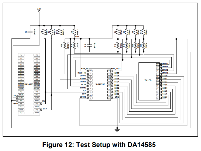
The GreenPAK can be controlled with any MCU capable of communicating with I2C commands. DA14585 is a Bluetooth 5.0 SOC-compliant chip capable of interfacing with the GreenPAK and LCD through I2C.
Figure 12 displays a schematic of the test setup with DA14585 chip powered from a 3.0V coin cell battery. P1_0 (Port 1 - Pin 0) and P1_1 (Port 1 – Pin 1) of the DA14585 are I2C pins for SDA and SCL respectively. SDA and SCL lines of the I2C are connected to the 3.0V rail using pull-up resistors R1 and R2. Please follow the description in 5.5 for writing data to the GreenPAK’s ASM RAM registers and I2C virtual inputs.
Similar system behavior was observed when using the DA14585 chip in place of the Arduino Uno to control the LCD. Some example code for controlling the LCD using the DA14585 is included in this ZIP file.
Conclusions
By using the GreenPAK solution described within this project, a system designer can decrease MCU pin count, decrease cost, increase system performance, and improve design flexibility. Additionally, battery-powered systems might benefit from reduced quiescent current consumption by implementing a low power mode to disable the LCD circuitry.
Oftentimes, MCUs are limited in their functionality based on the number of GPIOs provided to the designer. For smaller LCD applications, offloading LCD driving to the GreenPAK frees up numerous GPIO on the MCU at a low cost for the GreenPAK IC.
Similarly, MCUs are limited in their processing capabilities. Many modern MCUs utilize event-based programming to prioritize tasks in their specific programming environment. The GreenPAK solution allows MCUs to simplify their software requirements by sending a few I2C commands to each event. This allows the MCU firmware to either perform other tasks or put the MCU into a low power setting until an event is triggered in the system.
A native benefit of using the GreenPAK IC is the simplicity of testing and modifying designs within the GreenPAK Designer software. At the click of a few buttons, the RAM settings within the ASM and the oscillator clock speed can be changed. Similarly, the watchdog settings and the hardware reset timers can be configured within the IC.
References:
1] GreenPAK Designer Software, Software Download and User Guide, Dialog Semiconductor
[2] AN-CM-276 System Monitor 4-MUX LCD Driver Solution.gp, GreenPAK Design File, Dialog Semiconductor
[3] GreenPAK Development Tools, GreenPAK Development Tools Webpage, Dialog Semiconductor
[4] GreenPAK Application Notes, GreenPAK Application Notes Webpage, Dialog Semiconductor
[5] SLG46537, Datasheet, Dialog Semiconductor
[6] AN-1092, I2C Controlled State Machine, Application Note, Dialog Semiconductor
[7] AN1447, Software Driver for 4-Multiplexed LCD with a Standard ST62, Application Note,
STMicroelectronics
[8] AN658, LCD Fundamentals and the LCD Driver Module of 8-Bit PIC Microcontrollers, Application Note, Microchip
[9] AN1428, LCD Biasing and Contrast Control Methods, Application Note, Microchip.
[10] Wikipedia Contributors, Liquid-Crystal Display, Wikipedia The Free Encyclopedia, Page Version ID: 860435172, 2018
[11] TB1098, Low Power Techniques for LCD Applications, Application Note, Microchip
[12] Segment LCD Displays: Avoiding Excessive DC Component, Journal Article, Focus LCDs